Design of an Oscillator Using CMOS Transconductance Amplifier
advertisement

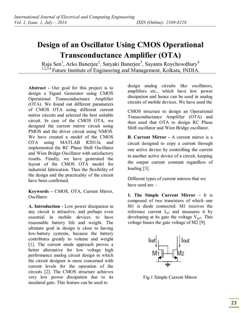
International Journal of Electrical and Computing Engineering Vol. 1, Issue. 1, July – 2014 ISSN (Online): 2349-8218 Design of an Oscillator Using CMOS Operational Transconductance Amplifier (OTA) Raja Sen1, Arko Banerjee2, Satyaki Banerjee3, Sayanta Roychowdhury4 1,2,3,4 Future Institute of Engineering and Management, Kolkata, INDIA. Abstract - Our goal for this project is to design a Signal Generator using CMOS Operational Transconductance Amplifier (OTA). We found out different parameters of CMOS OTA using different current mirror circuits and selected the best suitable circuit. In case of the CMOS OTA, we designed the current mirror circuit using PMOS and the driver circuit using NMOS. We have created a model of the CMOS OTA using MATLAB R2013a and implemented the RC Phase Shift Oscillator and Wien Bridge Oscillator with satisfactory results. Finally, we have generated the layout of the CMOS OTA model for industrial fabrication. Thus the flexibility of the design and the practicality of the circuit have been confirmed. Keywords – CMOS, OTA, Current Mirror, Oscillator. A. Introduction - Low power dissipation in any circuit is attractive, and perhaps even essential in mobile devices to have reasonable battery life and weight. The ultimate goal in design is close to having low-battery systems, because the battery contributes greatly to volume and weight [1]. The current mode approach proves a better alternative for low voltage high performance analog circuit design in which the circuit designer is more concerned with current levels for the operation of the circuits [2]. The CMOS structure achieves very low power dissipation due to its insulated gate. This feature can be used to design analog circuits like oscillators, amplifiers etc., which have low power dissipation and hence can be used in analog circuits of mobile devices. We have used the CMOS structure to design an Operational Transconductance Amplifier (OTA) and then used that OTA to design RC Phase Shift oscillator and Wien Bridge oscillator. B. Current Mirror - A current mirror is a circuit designed to copy a current through one active device by controlling the current in another active device of a circuit, keeping the output current constant regardless of loading [3]. Different types of current mirrors that we have used are – 1. The Simple Current Mirror – It is composed of two transistors of which one M1 is diode connected. M1 receives the reference current Iref and measures it by developing at its gate the voltage Vgs1. This voltage biases the gate voltage of M2 [9]. Fig.1 Simple Current Mirror 23 International Journal of Electrical and Computing Engineering Vol. 1, Issue. 1, July – 2014 ISSN (Online): 2349-8218 2. The Wilson Current Mirror – The relatively low value of the output resistance of the simple current mirror can be improved with the Wilson scheme shown in the figure. The gate to source voltage M1 to M2 is equal, therefore ensuring similar operation to the circuit. However we see that the addition of M3 and the established local feedback allow us to increase the output resistance [9]. result as equal. The addition of transistor M4 slightly changes the output resistance small signal analysis. The transistor M4, diode connected, adds a resistance 1/gm4 in series 4. The Cascode Current Mirror – An alternative way to increase the output resistance is to use the cascode configuration. The output stage consists of two transistors M2 and M3 in the cascode arrangement [11]. Their biases result from two other transistors M1 and M4 which are diode connected. Again, as for the previously stated current mirror the Vgs voltage of M1 and M2 are set equal. Therefore a replica of current in M1 is generated by M2. The output resistance increases because of the cascode arrangement [11]. Fig.2 Wilson Current Mirror 3. The Improved Wilson Current Mirror – The systematic current mismatch in the Wilson current mirror in compensated by the improved solution shown in the figure. One additional transistor is used, M4 which shifts down the voltage of the gate transistor M3 [4]. Therefore, the drain voltage of M1 is given by Vds1=Vgs3+Vds2-Vgs4 Fig.4 Cascode Current Mirror If the gate to source voltage of M3 and M4 are equal, the Vds voltage of M1 and M2 will with the resistance, Rl of the reference current. 24 International Journal of Electrical and Computing Engineering Vol. 1, Issue. 1, July – 2014 ISSN (Online): 2349-8218 Fig.5 Ideal OTA CMOS is an electronic device with high noise immunity and low static power consumption. CMOS also allows a high density of logic functions on a chip. It was primarily for this reason that CMOS became the most used technology to be implemented in VLSI chips [6]. Here the P Channel MOSFETs of the current mirror along with the N Channel MOSFETs of the driver circuit constitute the CMOS Operational Transconductance Amplifier [7]. Here port 1 is the non-inverting terminal and port 3 is the inverting terminal of the CMOS OTA. The output port is port 2. Since there is no existence of constant current source practically, so we have used a NMOS with Vgs=Vds such that the NMOS is in saturation [8]. This acts as a constant current source as the current through the NMOS is constant and independent of the voltage across it. Fig.3 Improved Wilson Current Mirror C. CMOS OTA - An OTA is a voltage controlled current source, more specifically the term “operational” comes from the fact that it takes the difference of two voltages as the input for the current conversion. The ideal transfer characteristic is therefore, Iout = gm. (Vin+ − Vin−) = gm.Vin where gm is the transconductance. An ideal OTA has infinite impedance (i.e. there is no input current). The common mode input range is also infinite, while the differential signal between these two inputs is used to control an ideal current source (i.e. the output current does not depend on the output voltage) that functions as an output. [5 & 10]. Parameter Current Input Output CMRR Bandwidth Slew Unity Gain Offset Offset (dB) (Hz) Bandwidth Voltage Voltage Rate (V/µs) Mirrors Product (Hz) SIMPLE 0.005pV -220.4nV 141.2 15.85M 77.23 15.85M WILSON 9.242mV -9.924mV 14.98 15.9K 101 15.9K IMPROVED 10pV 86.60nV 3.94 3.95M 0.09 3.95M 0.001pV 52.15nV 154.17 8M 80.35 8M WILSON CASCODE 25 International Journal of Electrical and Computing Engineering Vol. 1, Issue. 1, July – 2014 ISSN (Online): 2349-8218 for calculating different parameters. The results that we have got are shown in the table below. Fig.7 Frequency Response Curve using Cascode Current Mirror Fig.6 CMOS OTA D. Comparative Study of CMOS OTA using different current mirrors – We obtained different parameters like Output offset voltage, Input offset voltage, CMRR, Slew Rate, frequency response, unity gain bandwidth using different current mirrors. We changed the inputs to the driver circuit Fig.8 Output Plot of Slew Rate using Cascode Current Mirror Thus by analyzing all the parameters for different configurations of the current mirror circuit we can conclude that the CMOS OTA using Cascode Current mirror circuit offers best performance and is suitable for operations required for the intention of our project, which is to design a signal generator using CMOS OTA. 26 International Journal of Electrical and Computing Engineering Vol. 1, Issue. 1, July – 2014 ISSN (Online): 2349-8218 Fig.9 CMOS OTA using Cascode Current Mirror Fig.10 Layout of CMOS OTA using Cascode Current Mirror 2. Wien Bridge Oscillator - E. Oscillator using CMOS OTA 1. RC Phase Shift Oscillator - Fig.13 Wien Bridge Oscillator using CMOS OTA Fig.11 RC Phase Shift Oscillator using CMOS OTA 27 International Journal of Electrical and Computing Engineering Vol. 1, Issue. 1, July – 2014 ISSN (Online): 2349-8218 This is the schematic diagram of the RC phase shift oscillator using CMOS OTA. The CMOS OTA shown in the circuit is nothing but the CMOS OTA using Cascode Current Mirror. The components values that we have used here are Resistor3 =1.5 MΩ, Resistor2 = 100Ω, Resistor1 = Resistor4 = Resistor5 = R=10KΩ, Capacitor = C = 10nF. From the diagram shown above it is very clear that the components required in this type of oscillator are less compared to that of RC phase shift oscillator. The Wien bridge network is connected to the positive terminal of the CMOS OTA. The component values that we have used here are Resistor3 = 3KΩ, Resistor1 = 1KΩ, Resistor2 = Resistor4 = R = 10KΩ Capacitor3 = Capacitor1 = C = 16nF fo = Wo/2π = 1/2π.√6.RC fo = Wo/2π = 1/2π.RC Putting the values of R and C in the above equation we get f0 = 649 Hz. Practically, we get the oscillation frequency to be near about 600 Hz. So we can say the value that we got is close to the ideal value. Putting the values of R and C we get the oscillation frequency 994.72 Hz. Practically, we get the value of oscillation frequency 850 Hz approximately. F. Results and Discussion –We can observe Fig.12 Output of RC Phase Shift that calculated frequency Oscillator and frequency from graph are different. This is due to the lack of any frequency measurement tool in the Simulink file that we have used to design the wave generator. We had to calculate it from the output curve manually. This caused some discrepancy. The bandwidth that we got is 8MHz which is very high compared to the traditional OP-AMP (LM 741) which has 1.5MHz bandwidth. Moreover the slew rate is also very high in case of CMOS OTA using Cascode current mirror, 80.35 V/µs whereas in case of OP-AMP it is 0.7 V/µs [12]. The objective of our project was to create a functional OTA using CMOS and Fig.14 Output of Wien Bridge Oscillator use it to make a signal generator which can generate sine waveforms. We used Matlab R2013a to design the oscillator. We have also used Orcad Cadence version V16.0 to measure the various performance parameters of the CMOS OTA and also designed the layout of CMOS OTA using Microwind 3.1. References – [1] Design of A Low Voltage Low Power CMOS Current Mirror with Enhanced Dynamic Range, IJEAT Journal, Volume-2, Issue-3, February 2013. [2] Current Mode Computational Circuits for Analog Signal Processing, IJAREEIE, 28 International Journal of Electrical and Computing Engineering Vol. 1, Issue. 1, July – 2014 ISSN (Online): 2349-8218 Volume 3, Issue 4, April 2014. [3] Analysis and Design of Analog Integrated Circuits, 5th Edition by Paul Gray, Paul Hurst, Stephen Lewis, Robert Meyer. [4] A High Performance Novel PMOS Wilson Current Mirror, International Journal of Electronics Engineering. [5] Operational Transconductance Amplifier by Achim Gratz. [6] Transistor Level Implementation of CMOS Basic Gates in 0.18μm Technology, International Journal of Advanced Scientific and Technical Research Issue 3 volume 6, Nov.-Dec. 2013. [7] Basic Circuit Cells of Analog MOSFET Technology by Dr. John Choma. [8] Constant-Current Threshold Voltage Extraction in HSPICE for Nanoscale CMOS Analog Design by Alvin Loke presented at the Synopsys User Group (SNUG) San Jose 2010 Conference. [9] Bias circuit Outline CMOS by Alber Vargas [10] Active Filter Design Using Operational Transconductance Amplifiers: A Tutorial, IEEE Circuits and Devices Magazine, Vol.1, pp.20-32, March 1985. [11] Analog Design for CMOS VLSI Systems by Franco Malobert. [12] LM 741 Operational Amplifier, SNOSC25C by Texas Instruments–May 1998–Revised March 2013 29


