6484
CMOS Quad Rail-to-Rail
I/O Op Amp
V+
IN+D
IN+A
IN-A
OUT A
OUT D
IN-D
OUT B
OUT C
IN+C
V-
IN+B
IN-C
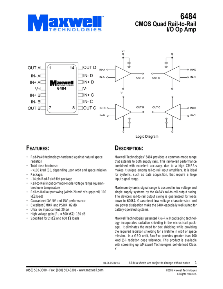
Logic Diagram
FEATURES:
DESCRIPTION:
• Rad-Pak® technology-hardened against natural space
radiation
• Total dose hardness:
- >100 krad (Si), depending upon orbit and space mission
• Package:
• - 14 pin Rad-Pak® flat package
• Rail-to-Rail input common-mode voltage range (guaranteed over temperature
• Rail-to-Rail output swing (within 20 mV of supply rail, 100
kΩ load)
• Guaranteed 3V, 5V and 15V performance
• Excellent CMRR and PSRR: 82 dB
• Ultra low input current: 20 pA
• High voltage gain (RL = 500 kΩ): 130 dB
• Specified for 2 kΩ and 600 Ω loads
Maxwell Technologies’ 6484 provides a common-mode range
that extends to both supply rails. This rail-to-rail performance
combined with excellent accuracy, due to a high CMRR<
makes it unique among rail-to-rail input amplifiers. It is ideal
for systems, such as data acquisition, that require a large
input signal range.
Maximum dynamic signal range is assured in low voltage and
single supply systems by the 6484’s rail-to-rail output swing.
The device’s rail-to-rail output swing is guaranteed for loads
down to 600Ω. Guaranteed low voltage characteristics and
low power dissipation make the 6484 especially well-suited for
battery-operated systems.
Maxwell Technologies' patented RAD-PAK® packaging technology incorporates radiation shielding in the microcircuit package. It eliminates the need for box shielding while providing
the required radiation shielding for a lifetime in orbit or space
mission. In a GEO orbit, RAD-PAK provides greater than 100
krad (Si) radiation dose tolerance. This product is available
with screening up toMaxwell Technologies self-defined Class
K.
01.06.05 Rev 4
(858) 503-3300 - Fax: (858) 503-3301 - www.maxwell.com
All data sheets are subject to change without notice
1
©2005 Maxwell Technologies
All rights reserved.
Memory
IN-B
6484
CMOS Quad Rail-to-Rail I/O Op Amp
TABLE 1. PINOUT DESCRIPTION
PIN
SYMBOL
DESCRIPTION
1, 7, 8, 14
OUT A-D
2, 6, 9, 13
IN- A-D
Negative Input Signal
3, 5, 10, 12
IN+ A-D
Positive Input Signal
4
V+
Positive Voltage
11
V-
Negative Voltage
Output Signal
TABLE 2. ABSOLUTE MAXIMUM RATINGS 1
PARAMETER
Supply Voltage (V+ - V-)
MIN
MAX
UNIT
VSS
--
16
V
-VSS
VSS
V
(V-) -0.3
(V+) +0.3
V
-5
5
mA
-30
30
mA
--
40
mA
Differential Input Voltage
Voltage at I/O Pin
Current at Input Pin
2
Current at Output Pin
3,4
Current at Power Supply Pin
Maximum Junction Temperature
TJ
--
150
°C
Power Dissipation
PD
--
315
mW
Storage Temperature Range
TS
-65
150
°C
Operating Temperature Range
TA
-55
125
°C
Lead Temperature (soldering 10 seconds)
--
260
°C
ESD Tolerance 5
--
2.0
kV
Memory
SYMBOL
1. Absolute Maximum Ratings indicate limits beyond which damage to the device may occur.
2. Limiting input pin current is only necessary for input voltages that exceed absolute maximum input voltage ratings.
3. Applies to both single-supply and split-supply operation. Continuous short circuit operation at elevated ambient temperature
can result in exceeding the maximum allowed junction temperature of 150°C. Output currents in excess of ±30 mA over long
term may adversely affect reliability.
4. Do not short circuit output to V+, when V+ is greater than 13V or reliability will be adversely affected.
5. Human body model, 1.5 kΩ in series with 100 pF. All pins rated per method 3015.6 of MIL-STD-883. This is a Class 2 device
rating.
TABLE 3. DELTA LIMITS
PARAMETER
VARIATION
ICC
±10% of specified value in Table 5
01.06.05 Rev 4
All data sheets are subject to change without notice
2
©2005 Maxwell Technologies
All rights reserved.
6484
CMOS Quad Rail-to-Rail I/O Op Amp
TABLE 4. RECOMMENDED OPERATING CONDITIONS
PARAMETER
Supply Voltage
SYMBOL
MIN
MAX
UNIT
VSS
3.0
15.5
V
TABLE 5. DC ELECTRICAL CHARACTERISTICS
(V+ = 5V, V- = 0V, R1 > 1MΩ, VCM = VO = V+/2, TA = -55 TO 125°C, UNLESS OTHERWISE SPECIFIED)
PARAMETER
Input Offset Voltage
Input Bias Current
Input Offset Current
TEST CONDITIONS
MIN
MAX
UNIT
VIO
25°C
--
0.75
mV
-55 TO 125°C
--
1.35
25°C
--
25
-55 TO 125°C
--
100
25°C
--
25
-55 TO 125°C
--
100
25°C
65
--
-55 TO 125°C
62
--
25°C
65
--
-55 TO 125°C
62
--
25°C
65
--
-55 TO 125°C
62
--
25°C
65
--
-55 TO 125°C
62
--
25°C
(V+) + 0.25
-0.25
-55 TO 125°C
V+
0
25°C
16
--
-55 TO 125°C
12
--
25°C
11
--
-55 TO 125°C
9
--
25°C
28
--
-55 TO 125°C
22
--
25°C
30
--
-55 TO 125°C
24
--
25°C
--
2.8
-55 TO 125°C
--
3.6
25°C
--
3.0
-55 TO 125°C
--
4.0
IIB
IIO
CMRR
0V < VCM < 15V, V+ = 15V
0V < VCM < 5V
Positive Power Supply
Rejection Ratio
+PSRR
Negative Power Supply
Rejection Ratio
-PSRR
Input Common Mode
Voltage Range
VCM
Output Short Circuit
Current
ISC
5V < V+ <15V, VO = 2.5V
-5V < V- < -15V, VO = -2.5V, V+ = 0V
5V > VCM > 15V, For CMRR > 50 dB
Sourcing, VO = 0V
Sinking, VO = 5V
V+ = 15V, Sourcing, VO = 0V
V+ = 15V, Sinking, VO = 12V
Supply Current
ICC
All four amps
All four amps, V+ = 15V
01.06.05 Rev 4
1
pA
pA
Memory
Common Mode
Rejection Ratio
SYMBOL
dB
dB
dB
V
mA
mA
All data sheets are subject to change without notice
3
©2005 Maxwell Technologies
All rights reserved.
6484
CMOS Quad Rail-to-Rail I/O Op Amp
TABLE 5. DC ELECTRICAL CHARACTERISTICS
(V+ = 5V, V- = 0V, R1 > 1MΩ, VCM = VO = V+/2, TA = -55 TO 125°C, UNLESS OTHERWISE SPECIFIED)
PARAMETER
Output Swing
SYMBOL
VO
TEST CONDITIONS
V+ = 5V, R1 = 2 kΩ to V+/2
V+ = 5V, R1 = 600 Ω to V+/2
V+ = 15V, R1 = 2 kΩ to V+/2
V+ = 15V, R1 = 600 Ω to V+/2
Large Signal Voltage
Gain 2
R1 = 2 kΩ Sourcing
AV
R1 = 2 kΩ Sinking
R1 = 600 Ω Sinking
MAX
UNIT
25°C
4.8
0.18
V
-55 TO 125°C
4.7
0.24
25°C
4.5
0.50
-55 TO 125°C
4.24
0.65
25°C
14.4
0.32
-55 TO 125°C
14.2
0.45
25°C
13.4
1.00
-55 TO 125°C
13.0
1.3
25°C
140
--
-55 TO 125°C
84
--
25°C
35
--
-55 TO 125°C
20
--
25°C
80
--
-55 TO 125°C
48
--
25°C
18
--
-55 TO 125°C
13
--
V/mV
Memory
R1 = 600 Ω Sourcing
MIN
1. Do not short circuit output to V+, when V+ is greater than 13V or reliability will be adversely affected.
2. V+ = 15V, VCM = 7.5V and R1 connected to 7.5V. For sourcing tests, 7.5V < VO < 11.5V. For sinking tests, 3.5V < VO < 7.5V.
TABLE 6. AC PARAMETER
(V+ = 5V, V- = 0V, R1 > 1MΩ, VCM = VO = V+/2, TA = -55 TO 125°C, UNLESS OTHERWISE SPECIFIED)
PARAMETER
SYMBOL
Slew Rate 1
SR
Gain Bandwidth
GBW
TEST CONDITIONS
V+ = 15V, set up for non-inverting
MIN
MAX
UNIT
0.9
0.6
---
V/µ S
1.25
1.15
---
MHz
1. V+ = 15V. Connected as Voltage Follower with 10V step input, 2.5V to 12.5V for +Slew, and 12.5V to 2.5V for (-)Slew. Number
specified is the slower of either the positive or negative slew rates.
01.06.05 Rev 4
All data sheets are subject to change without notice
4
©2005 Maxwell Technologies
All rights reserved.
6484
CMOS Quad Rail-to-Rail I/O Op Amp
Memory
14 PIN RAD-PAK® FLAT PACKAGE
SYMBOL
DIMENSION
MIN
NOM
MAX
A
0.140
0.157
0.170
b
0.015
0.017
0.020
c
0.004
0.005
0.009
D
--
0.380
0.390
E
0.250
0.255
0.260
E1
--
--
0.290
E2
0.125
0.130
--
E3
0.030
0.062
--
e
0.050 BSC
L
0.270
0.325
0.370
Q
0.026
0.030
0.035
S1
0.005
--
--
N
14
Note: All dimensions in inches.
F14-05
01.06.05 Rev 4
All data sheets are subject to change without notice
5
©2005 Maxwell Technologies
All rights reserved.
CMOS Quad Rail-to-Rail I/O Op Amp
6484
Important Notice:
These data sheets are created using the chip manufacturer’s published specifications. Maxwell Technologies verifies
functionality by testing key parameters either by 100% testing, sample testing or characterization.
The specifications presented within these data sheets represent the latest and most accurate information available to
date. However, these specifications are subject to change without notice and Maxwell Technologies assumes no
responsibility for the use of this information.
Maxwell Technologies’ products are not authorized for use as critical components in life support devices or systems
without express written approval from Maxwell Technologies.
Any claim against Maxwell Technologies must be made within 90 days from the date of shipment from Maxwell Technologies. Maxwell Technologies’ liability shall be limited to replacement of defective parts.
Memory
01.06.05 Rev 4
All data sheets are subject to change without notice
6
©2005 Maxwell Technologies
All rights reserved.
6484
CMOS Quad Rail-to-Rail I/O Op Amp
Product Ordering Options
Model Number
6484
RP
F
X
Option Details
Feature
Screening Flow
Monolithic
K = Maxwell Self-Defined Class K1
H = Maxwell Self-Defined Class H1
I = Industrial (testing @ -55°C,
+25°C, +125°C)
E = Engineering (testing @ +25°C)
F = Flat Pack
Radiation Feature
RP = RAD-PAK® package
Base Product
Nomenclature
CMOS Quad Rail-to-Rail I/O OpAmp
Memory
Package
1)Products are manufactured and screened to Maxwell Technologies self-defined Class H and Class K flows.
01.06.05 Rev 4
All data sheets are subject to change without notice
7
©2005 Maxwell Technologies
All rights reserved.
