ISL97701
Data Sheet
February 22, 2008
Boost Regulator with Integrated Schottky
and Input Disconnect Switch
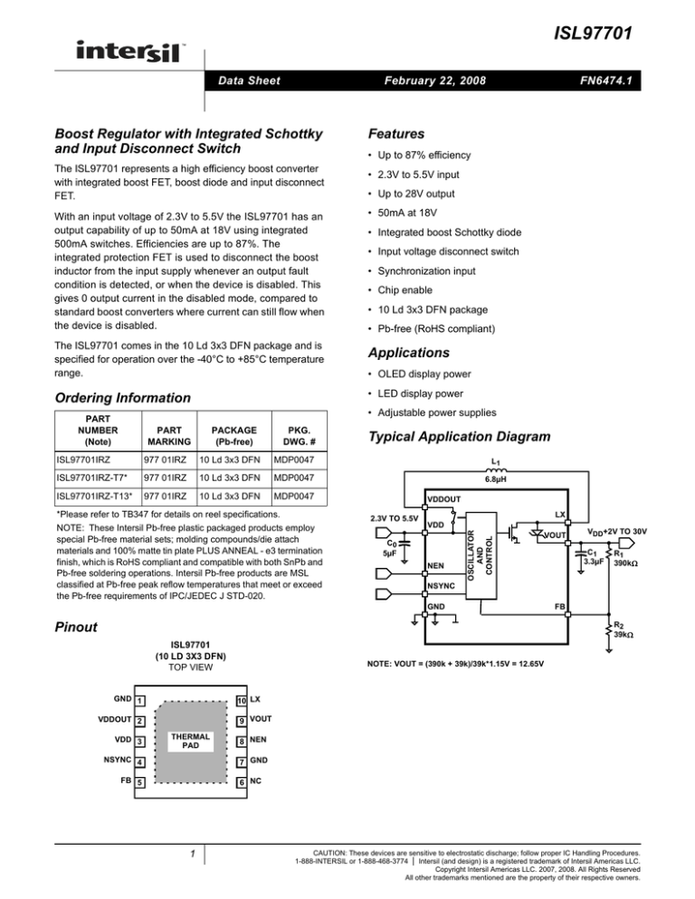
The ISL97701 represents a high efficiency boost converter
with integrated boost FET, boost diode and input disconnect
FET.
With an input voltage of 2.3V to 5.5V the ISL97701 has an
output capability of up to 50mA at 18V using integrated
500mA switches. Efficiencies are up to 87%. The
integrated protection FET is used to disconnect the boost
inductor from the input supply whenever an output fault
condition is detected, or when the device is disabled. This
gives 0 output current in the disabled mode, compared to
standard boost converters where current can still flow when
the device is disabled.
The ISL97701 comes in the 10 Ld 3x3 DFN package and is
specified for operation over the -40°C to +85°C temperature
range.
FN6474.1
Features
• Up to 87% efficiency
• 2.3V to 5.5V input
• Up to 28V output
• 50mA at 18V
• Integrated boost Schottky diode
• Input voltage disconnect switch
• Synchronization input
• Chip enable
• 10 Ld 3x3 DFN package
• Pb-free (RoHS compliant)
Applications
• OLED display power
• LED display power
Ordering Information
• Adjustable power supplies
PART
NUMBER
(Note)
PART
MARKING
PACKAGE
(Pb-free)
PKG.
DWG. #
Typical Application Diagram
ISL97701IRZ
977 01IRZ
10 Ld 3x3 DFN
MDP0047
L1
ISL97701IRZ-T7*
977 01IRZ
10 Ld 3x3 DFN
MDP0047
6.8µH
ISL97701IRZ-T13*
977 01IRZ
10 Ld 3x3 DFN
MDP0047
NOTE: These Intersil Pb-free plastic packaged products employ
special Pb-free material sets; molding compounds/die attach
materials and 100% matte tin plate PLUS ANNEAL - e3 termination
finish, which is RoHS compliant and compatible with both SnPb and
Pb-free soldering operations. Intersil Pb-free products are MSL
classified at Pb-free peak reflow temperatures that meet or exceed
the Pb-free requirements of IPC/JEDEC J STD-020.
2.3V TO 5.5V
LX
VDD
C0
5µF
NEN
OSCILLATOR
AND
CONTROL
*Please refer to TB347 for details on reel specifications.
VDDOUT
VOUT
VDD+2V TO 30V
C1
3.3µF
R1
390k
NSYNC
GND
FB
R2
39k
Pinout
ISL97701
(10 LD 3X3 DFN)
TOP VIEW
GND 1
10 LX
9 VOUT
VDDOUT 2
VDD 3
NOTE: VOUT = (390k + 39k)/39k*1.15V = 12.65V
THERMAL
PAD
NSYNC 4
8 NEN
7 GND
FB 5
6 NC
1
CAUTION: These devices are sensitive to electrostatic discharge; follow proper IC Handling Procedures.
1-888-INTERSIL or 1-888-468-3774 | Intersil (and design) is a registered trademark of Intersil Americas LLC.
Copyright Intersil Americas LLC. 2007, 2008. All Rights Reserved
All other trademarks mentioned are the property of their respective owners.
ISL97701
Block Diagram
VDD
SYNCHRONIZATION
SIGNAL DETECTOR
UNDERVOLTAGE
DETECTOR
OVER-TEMPERATURE
DETECTOR
1
NSYNC
OVERCURRENT
DETECTOR (DC)
MUX
0
OSCILLATOR
VDD
CLK
NEN
START
GND
ERROR
AMP
+
FB
VDD
RESTART DISABLE AND WAIT
STATE MACHINE
(DEFAULT SEQUENCE)
1. SOFT INRUSH
2. VDDOUT ENABLE
3. SOFT BOOST 25
4. SOFT BOOST 50
5. SOFT BOOST 75
6. NORMAL
SLOPE
COMPENSATION
RAMP-GENERATOR
CCOMP CLAMP
S2
VDDOUT
OVERVOLTAGE
DETECTOR
2
+
As
+
Av
+
Ai
-
VOLTAGE
REFERENCE
LX
EN
CONTROL LOGIC
-PWM TIMING
-CURRENT LIMIT
-PULSE SKIPPING
VOUT
GATE
DRIVER
CURRENT
LIMIT
COMPARATOR
RSENSE
GND
ISL97701
FIGURE 1. ISL97701 BLOCK DIAGRAM
2
FN6474.1
February 22, 2008
ISL97701
Absolute Maximum Ratings (TA = +25°C)
Thermal Information
VDD to GND . . . . . . . . . . . . . . . . . . . . . . . . . . . . . . . . . . -0.3V to 6V
VOUT to GND. . . . . . . . . . . . . . . . . . . . . . . . . . . . . . . . . -0.3V to 31V
LX to GND . . . . . . . . . . . . . . . . . . . . . . . . . . . . . . . . . . . . VOUT + 1V
VDDOUT, NSYNC, FB, NEN
to GND . . . . . . . . . . . . . . . . . . . . . . . . . . . . . -0.3V to VDD + 0.3V
Continuous Current in VDD, GND, VDDOUT, LX . . . . . . . . . 650mA
Continuous Current in NSYNC, FB, NEN . . . . . . . . . . . . . . . . 10mA
Thermal Resistance (Typical, Notes 1, 2) JA (°C/W) JC (°C/W)
10 Ld 3x3 DFN Package . . . . . . . . . . .
48
7
Storage Temperature . . . . . . . . . . . . . . . . . . . . . . . .-65°C to +150°C
Ambient Operating Temperature (TA) . . . . . . . . . . . .-40°C to +85°C
Operating Junction Temperature (TJ) . . . . . . . . . . . . . . . . . . +125°C
Maximum Junction Temperature . . . . . . . . . . . . . . . . . . . . . . +130°C
Pb-free reflow profile . . . . . . . . . . . . . . . . . . . . . . . . . .see link below
http://www.intersil.com/pbfree/Pb-FreeReflow.asp
CAUTION: Do not operate at or near the maximum ratings listed for extended periods of time. Exposure to such conditions may adversely impact product reliability and
result in failures not covered by warranty.
NOTES:
1. JA is measured in free air with the component mounted on a high effective thermal conductivity test board with “direct attach” features. See
Tech Brief TB379.
2. For JC, the “case temp” location is the center of the exposed metal pad on the package underside.
Electrical Specifications
PARAMETER
VDD = 3.6V, GND = NEN = 0V, NSYNC = VDD, R1 = 390k, R2 = 39k, L = 10µH, TA = -40°C to +85°C unless
otherwise stated.
DESCRIPTION
CONDITION
MIN
TYP
MAX
UNIT
5.5
V
0.1
3
µA
250
350
k
1
µA
SUPPLY
VDD
Supply Operating Voltage Range
IDIS
Supply Current when Disabled
2.3
NEN = VDD
LOGIC INPUTS – NEN, NSYNC
RUP
Pull-up Resistor
Enabled, Input at GND
150
IIL
Leakage Current when Disabled
Disabled, Input at GND
-1
VHI
Logic High Threshold
VLO
Logic Low Threshold
1.8
V
0.7
V
2.3
V
POWER-ON RESET – VDD
VRES_ON
Power-On Reset Threshold
VDD rising
VRES_OFF
Power-Off Threshold
VDD falling
2.2
1.9
2
0.9
1
V
LX OUTPUT DRIVER
fOSC
LX Switching Frequency with Internal
Oscillator
fSYNC
LX Switching Frequency when
Externally Synchronized at NSYNC
tON-MIN
Minimum On-Time
FB = 0V, I(LX) > Ilim(LX)
60
ns
tOFF-MIN
Minimum Off-time
( Maximum Duty Cycle)
FB = 0V, I(LX) < Ilim(LX)
60
ns
rON
LX ON-Resistance
I(LX) = 100mA
0.4
ILEAK
LX Leakage Current
NEN = VDD, V(LX) = 30V
IPEAK
LX Peak Current Limit
t > 8.32ms (end of soft-start)
1.1
MHz
f
(NSYNC)
1
5
1200
µA
mA
SCHOTTKY DIODE – LX, VOUT
VDIODE
Forward Voltage from LX to VOUT
3
I = 10mA, TA = +25°C
0.4
0.5
0.6
V
I = 10mA, TA = -40°C to +85°C
0.3
0.5
0.7
V
FN6474.1
February 22, 2008
ISL97701
Electrical Specifications
PARAMETER
VDD = 3.6V, GND = NEN = 0V, NSYNC = VDD, R1 = 390k, R2 = 39k, L = 10µH, TA = -40°C to +85°C unless
otherwise stated. (Continued)
DESCRIPTION
CONDITION
MIN
TYP
MAX
UNIT
TA = +25°C
1.13
1.15
1.17
V
TA = -40°C to +85°C
1.12
1.15
1.18
V
-0.2
0.2
µA
25
1400
kHz
100
ns
FEEDBACK INPUTS
VrefFB
Input Reference Voltage on FB
IFB
Input Current in FB
FB = 1.3V
RFB
FB Pull-Down Switch Resistance
IFB = 10mA
15
SYNCHRONIZATION INPUT – NSYNC
fNSYNC
External Sync Frequency Range
tdNSYNC
NSYNC Falling Edge to LX Falling Edge
Delay
600
fNSYNC = 600kHz
80
OVERVOLTAGE DETECTOR - VOUT
VOUT
Overvoltage Threshold
FB = GND
31
35
V
t > 2.048ms, DC current
800
mA
OVERCURRENT DETECTOR
IOCTVDDOUT
Overcurrent Threshold
OVER-TEMPERATURE DETECTOR
tOFF
Shut-Down Temperature Threshold
T rising
135
°C
tON
Turn-On Temperature Threshold
T falling
100
°C
FAULT SWITCH – VDD, VDDOUT
rONFS
ON-Resistance from VDD to VDDOUT
IOUT = 50mA, t > 2.048ms
0.2
IleakVDDOUT
Leakage Current
VDDOUT = 0V
0.01
ISS_VDDOUT
Soft Inrush Current Source at VDDOUT
VDD - VDDOUT = 0.5V, tON < 2.048ms
Output Voltage Accuracy, Assuming
Resistor Divider Tolerances of 0.1% or
Better
IOUT = 10mA, TA = +25°C
-1.5
1.5
%
IOUT = 10mA, TA = -40°C to +85°C
-2.5
2.5
%
VOUT/IOUT
Load Regulation
IOUT = 0mA to 50mA
0.05
%
VOUT/VDD
Line Regulation
VDD = 3.6V to 2.6V, IOUT = 30mA
0.1
%/V
3
50
µA
mA
REGULATION
ACC
4
FN6474.1
February 22, 2008
ISL97701
Typical Performance Curves
90
90
4.2V
4.2V
85
80
EFFICIENCY (%)
EFFICIENCY (%)
85
3.6V
2.7V
75
2.7V
75
70
70
65
3.6V
80
65
0
50
100
150
0
50
100
150
IOUT (mA)
LOAD CURRENT (mA)
FIGURE 2. EFFICIENCY vs LOAD CURRENT (VOUT = 18.3V)
L = 10µH (CDRH4D28C-100NC) C = 6.6µF
FIGURE 3. EFFICIENCY vs IOUT (VOUT = 18.3V)
L = 6.8µH (TDK RLF7030) C = 6.6µF
90
90
4.2V
4.2V
85
EFFICIENCY (%)
EFFICIENCY (%)
85
3.6V
80
2.7V
75
70
65
3.6V
80
2.7V
75
70
0
50
100
150
200
65
0
50
FIGURE 4. EFFICIENCY vs IOUT (VOUT = 12.6V)
L = 6.8µH (TDK RLF7030) C = 6.6µF
V(NEN)
100
150
200
IOUT (mA)
IOUT (mA)
FIGURE 5. EFFICIENCY vs IOUT (VOUT = 12.7V)
L = 10µH (CDRH4D28C-100NC) C = 6.6µF
V(NEN)
V(VOUT)
V(VOUT)
I(VDD)
I(VDD)
FIGURE 6. START-UP TO 12V (VDD = 3.6V, RL = 360)
5
FIGURE 7. START-UP TO 18V (VDD = 3.6V, RL = 360)
FN6474.1
February 22, 2008
ISL97701
Typical Performance Curves
(Continued)
V(NEN)
18.20
18.19
18.18
18.17
VOUT (V)
V(VOUT)
18.16
18.15
18.14
18.13
18.12
18.11
18.10
18.09
I(VDD)
0
50
100
150
LOAD CURRENT (mA)
FIGURE 9. LOAD REGULATION (VIN = 3.6V)
FIGURE 8. SHUTDOWN (VDD = 3.6V, RL = 360)
18.29
QUIESCENT CURRENT (µA)
1200
18.28
VOUT (V)
18.27
18.26
18.25
18.24
18.23
2.6
3.1
3.6
4.1
4.6
1000
800
600
400
200
0
5.1
0
1
2
VIN (V)
3
4
5
6
VIN (V)
FIGURE 11. QUIESCENT CURRENT vs VIN
FIGURE 10. LINE REGULATION (IOUT = 30mA)
3.2
2.9
2.6
POUT (W)
2.3
2.0
1.7
1.4
1.1
0.8
(CH1 = VOUT; CH4 = iL; CH2 = IOUT)
FIGURE 12. TRANSIENT RESPONSE (VIN = 3.3V;
VOUT = 18.3V; STEP LOAD CURRENT FROM
2.6mA TO 70mA)
6
0.5
2.3
2.7
3.1
3.5
3.9
VIN (V)
4.3
4.7
5.1
5.5
FIGURE 13. RECOMMENDED MAXIMUM OUTPUT POWER vs
INPUT VOLTAGE
FN6474.1
February 22, 2008
ISL97701
When NEN is driven low the ISL97701 begins with the
start-up sequence.
Pin Descriptions
PIN
NUMBER
PIN NAME
1
GND
2
VDDOUT
3
VDD
4
NSYNC
5
FB
Feedback Input
6
NC
Do Not Connect
7
GND
Ground
8
NEN
Enable Input (Active Low)
SOFT INRUSH: STATE DURATION ~2.048ms
9
VOUT
Boost Output Voltage
10
LX
The switch at VDDOUT is configured as current source and
provides a limited current through the inductor to pre-charge
the capacitor at VOUT.
PIN FUNCTION
Start-Up Sequence
Ground
Protection Switch Output
Supply Input
Synchronization Input (Falling Edge)
If the sequence has completed, the ISL97701 stays in the
“Normal” state until NEN is high again or any fault is detected.
Boost FET
Function Overview
The ISL97701 is a high frequency, high efficiency boost
regulator which operates in constant frequency PWM mode.
The boost converter generates a stable, higher output
voltage from a variable, low voltage input source (e.g. Li-ion
battery). The output voltage level is defined from the
feedback resistor network in Equation 1.
V OUT = V refFB R 1 + R 2 R 2
After pin NEN is pulled low or a restart is triggered from Fault
Control during operation, the ISL97701 goes through a startup sequence with the following six states: Soft Inrush ->
VDDOUT Enable -> Soft Boost 25 -> Soft Boost 50 -> Soft
Boost 75 -> Normal.
(EQ. 1)
The switching frequency is either generated from the fixed
1MHz internal oscillator or provided externally at the
synchronization pin in the range from 600kHz to 1.4MHz.
The compensation network and soft-start functions are built
in with fixed parameters without any need for further external
components.
To stop battery discharge into the output load when disabled,
the inductor is disconnected from the input supply with a low
ON-resistance power switch.
VDDOUT ENABLE: STATE DURATION ~128Μs
The switch at VDDOUT is fully enabled and connects the
inductor to VDD with a low ON-resistance.
SOFT BOOST 25 -> 50 -> 75: STATE DURATION
3x ~2.048ms
The boost regulator begins to switch at LX.
The LX current limit increases in three steps representing
25%, 50% and 75% of its final value.
NORMAL
If no fault was detected Normal state is entered ~8.256ms
after NEN is pulled low.
The LX current limit steps up to 100%.
In all states Fault Control can force the sequence to restart
or even to shutdown (see Table 1).
V(NEN)
Built-in fault protection monitors inductor current and output
voltage as well as junction temperature in order to interrupt
the high current circuit path through the inductor and diode in
the event of a load failure.
V(VOUT)
Low logic input thresholds allow the ISL97701 to interface
directly to microcontrollers with lower supply voltage.
Alternatively, the internal pull-up resistors on all logic inputs
provide level shifting when driven from open collector outputs.
Description of Operation
NORMAL
75
SOFT
INRUSH
Enable Pin (Active Low) - NEN
If NEN is high, the ISL97701 shuts down all its internal
functions and deactivates its I/So. Only the internal pull-up
resistor at NEN remains active. If NEN is high, the input
disconnect switch between VDD and VDDOUT interrupts the
circuit path from the input voltage VDD through inductor and
diode to the output load at VOUT. If shutdown, the total
supply current in VDD is typically less than 0.1µA.
7
I(VDD)
50
25
VDDOUT ENABLE
FIGURE 14. FAULT CONTROL SEQUENCE
Fault Control
The input voltage at VDD, current in the VDDOUT switch,
voltage at VOUT and junction temperature TJ are
continuously monitored and can either restart the start-up
FN6474.1
February 22, 2008
ISL97701
sequence or in some cases disable the ISL97701 boost
function as long as the fault is present.
TABLE 1. FAULT PROTECTION
FAULT
DESCRIPTION
FAULT
CONDITION
ISL97701 FAULT REACTION
Undervoltage at
VDD
V(VDD) <
V(VDD)off
Overcurrent
drawn from
VDDOUT
I(VDDOUT) > Disables VDDOUT switch and
It(VDDOUT)err LX driver and immediately
restarts the start-up sequence
Overvoltage at
VOUT
V(VOUT) >
Vt(VOUT)err
Disables I/Os and waits until
V(VDD) reaches V(VDD)on to
begin with the start-up sequence
pin is, for example, static high, the internal oscillator defines
the LX output frequency and phase. When externally
synchronized, all falling edges at LX are timed from the
falling edge of the clock signal applied at NSYNC. The timing
of the rising edge at LX is defined by the boost controller.
V(NSYNC)
Disables VDDOUT switch and
LX driver and waits until output
voltage V(VOUT) drops to
Vt(VOUT) to restart the start-up
sequence
Over-Temperature Tj > Toff
on chip
Disables VDDOUT switch and
LX driver and waits until junction
temp drops to “Ton” to restart the
start-up sequence
V(LX)
FIGURE 15. NSYNC TO LX SYNCHRONIZATION DELAY
Maximum Duty Cycle – LX
The maximum duty cycle Dmax, at which the power FET can
operate defines the upper limit of the regulator output to
input voltage ratio according to Equation 2:
V OUT
1
---------------- = -------------------------1 – DMAX
V IN
V(NSYNC)
(EQ. 2)
In the ISL97701, DMAX is defined from the minimum off-time
tOFF(LX)min and the switching frequency.
V(LX)
If NSYNC is tied to VDD the internal oscillator defines DMAX
according to Equation 3:
D MAX f OSC = 1 – t OFF LX min f OSC
(EQ. 3)
With external synchronization at pin NSYNC:
D MAX NSYNC = 1 – t OFF LX min f NSYNC
(EQ. 4)
The duty cycle at LX can be 0% (pulse skipping), if the
output voltage exceeds the target voltage set with the
feedback resistors.
FIGURE 16. LX SYNCHRONIZATION WITH f(SYNC) = 600kHz
V(NSYNC)
Internal Schottky Diode – LX, VOUT
The inductor node LX internally connects to the power FET
and to the anode of the integrated power Schottky diode.
The cathode of the diode is pin VOUT. An overvoltage
detector at VOUT continuously monitors the cathode voltage
and immediately disables the boost regulator if the voltage
exceeds the maximum allowable voltage.
V(LX)
External Synchronization Pin - NSYNC
Pin NSYNC can be used to synchronize the LX output pin with
an external clock signal in the range from 600kHz to 1.4MHz.
A frequency detector monitoring NSYNC enables external
synchronization if f(NSYNC) is higher than ~300kHz. If the
8
FIGURE 17. LX SYNCHRONIZATION WITH f(SYNC) = 1.4MHz
FN6474.1
February 22, 2008
ISL97701
C7
3.3µF/50V
R1
390k
J7
VOUT
C6
1nF/50V
C8
100nF
L1
J2
J3
6.8µH
U1
VDD_IN
J4
2
VDD
J1
3
C1
VDD 100nF
C2
10µF
4
C9
4.7µF/10V
5
R6
39k
LX 10
VDDOUT
9
VOUT
VDD
8
NEN
NSYNC
7
GND
FB
6
NC
GND
R3
OPEN
GND_OUT
VDD
1
1
J1 2
J6
NEN
3
GND_IN
ISL97701
JP3
NSYNC
FIGURE 18. ISL97701 APPLICATION BOARD
Typical Application
Typical applications are passive- or active-matrix organic
light emitting diode displays (PMOLED, AMOLED) in
handheld devices. Applications with low power or screen
saver mode is directly supported.
TABLE 2. OPTIMAL COMBINATION OF BOOST INDUCTOR L
AND OUTPUT CAPACITOR COUT
CAPACITOR (µF)
INDUCTOR (µH)
MIN
MAX
4.7
2.2
10
6.8
3.3
10
10
4.7
10
15
6.8
10
Components Selection
The input capacitance is normally 10µf~15µF and the output
capacitor is 3.3µf to 6.6µF. X5R or X7R type of ceramic
capacitor with correct voltage rating is recommended. The
output capacitor value will affect the output voltage ripple.
The higher the value of the output capacitor, the lower the
ripple of the output voltage.
When choosing an inductor, make sure the inductor can
handle the average and peak currents given by Equations 5,
6 and 7 (80% efficiency assumed):
I OUT V OUT
I LAVG = ---------------------------------0.8 V IN
(EQ. 5)
1
I LPK = I LAVG + --- I L
2
(EQ. 6)
V IN V OUT – V IN
I L = --------------------------------------------------L V OUT f OSC
(EQ. 7)
Where:
• IL is the peak-to-peak inductor current ripple in Amperes
• L is the inductance in H
• fOSC is the switching frequency, typically 1.0MHz
Optimal combinations of the boost inductor L and the output
capacitor COUT are listed in Table 2:
9
Recommended inductor and ceramic capacitor
manufacturers are listed in Table 3:
TABLE 3. RECOMMENDED INDUCTOR AND CERAMIC
CAPACITOR MANUFACTURERS
INDUCTOR
CERAMIC CAPACITOR
Sumida: www.sumida.com
Taiyo Yuden: www.t-yuden.com
TDK:
www.tdk.co.jp
AVX:
www.avxcorp.com
Toko:
www.tokoam.com
Murata:
www.murata.com
PCB Layout Considerations
The layout is very important for the converter to function
properly. To ensure the high pulse current in the power
ground does not interfere with the sensitive feedback
signals, the current loops (VIN-L1-LX-GND, and VIN-L1VOUT-COUT-GND) should be as short as possible. For the
DFN package, there is no separated GND. All return GNDs
should be connected in GND pin but with no sharing branch.
The heat of the IC is mainly dissipated through the thermal
pad. Maximizing the copper area connected to the thermal
pad is preferable. In addition, a solid ground plane is helpful
for the EMI performance.
FN6474.1
February 22, 2008
ISL97701
Dual Flat No-Lead Package Family (DFN)
MDP0047
A
DUAL FLAT NO-LEAD PACKAGE FAMILY (JEDEC REG: MO-229)
D
MILLIMETERS
N N-1
0.075 C
2X
PIN #1
I.D.
E
1
2
0.075 C
B
2X
TOP VIEW
(D2)
4
L1
N-1
N
L
(N LEADS)
SYMBOL
DFN8
DFN10
TOLERANCE
A
0.85
0.90
±0.10
A1
0.02
0.02
+0.03/-0.02
b
0.30
0.25
±0.05
c
0.20
0.20
Reference
D
4.00
3.00
Basic
D2
3.00
2.25
Reference
E
4.00
3.00
Basic
E2
2.20
1.50
Reference
e
0.80
0.50
Basic
L
0.50
0.50
±0.10
L1
0.10
0
Maximum
Rev. 2 2/07
NOTES:
(E2)
1. Dimensioning and tolerancing per ASME Y14.5M-1994.
PIN #1 I.D.
1
2
5
3
e
b
0.10 M C A B
3. Bottom-side pin #1 I.D. may be a diepad chamfer, an extended
tiebar tab, or a small square as shown.
4. Exposed leads may extend to the edge of the package or be
pulled back. See dimension “L1”.
5. Inward end of lead may be square or circular in shape with radius
(b/2) as shown.
BOTTOM VIEW
0.10
2. Exposed lead at side of package is a non-functional feature.
6. N is the total number of leads on the device.
C
C
SEATING
PLANE
0.08
C
SEE DETAIL "X"
(N LEADS
& EXPOSED PAD)
2
C
A
(c)
A1
DETAIL X
All Intersil U.S. products are manufactured, assembled and tested utilizing ISO9001 quality systems.
Intersil Corporation’s quality certifications can be viewed at www.intersil.com/design/quality
Intersil products are sold by description only. Intersil Corporation reserves the right to make changes in circuit design, software and/or specifications at any time without
notice. Accordingly, the reader is cautioned to verify that data sheets are current before placing orders. Information furnished by Intersil is believed to be accurate and
reliable. However, no responsibility is assumed by Intersil or its subsidiaries for its use; nor for any infringements of patents or other rights of third parties which may result
from its use. No license is granted by implication or otherwise under any patent or patent rights of Intersil or its subsidiaries.
For information regarding Intersil Corporation and its products, see www.intersil.com
10
FN6474.1
February 22, 2008
