JW3310
4-Cell Battery Monitoring IC
With 3.3V LDO Output
Parameters Subject to Change Without Notice
DESCRIPTION
FEATURES
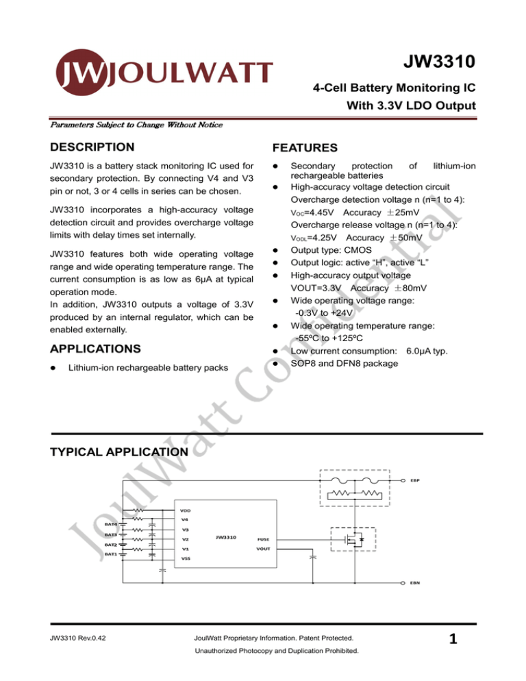
JW3310 is a battery stack monitoring IC used for
secondary protection. By connecting V4 and V3
pin or not, 3 or 4 cells in series can be chosen.
±
±
JW3310 incorporates a high-accuracy voltage
detection circuit and provides overcharge voltage
limits with delay times set internally.
JW3310 features both wide operating voltage
range and wide operating temperature range. The
current consumption is as low as 6µA at typical
operation mode.
In addition, JW3310 outputs a voltage of 3.3V
produced by an internal regulator, which can be
enabled externally.
APPLICATIONS
Lithium-ion rechargeable battery packs
Secondary
protection
of
lithium-ion
rechargeable batteries
High-accuracy voltage detection circuit
Overcharge detection voltage n (n=1 to 4):
VOC=4.45V Accuracy
25mV
Overcharge release voltage n (n=1 to 4):
VODL=4.25V Accuracy
50mV
Output type: CMOS
Output logic: active “H”, active “L”
High-accuracy output voltage
VOUT=3.3V Accuracy 80mV
Wide operating voltage range:
-0.3V to +24V
Wide operating temperature range:
-55ºC to +125ºC
Low current consumption: 6.0µA typ.
SOP8 and DFN8 package
±
TYPICAL APPLICATION
JW3310 Rev.0.42
JoulWatt Proprietary Information. Patent Protected.
Unauthorized Photocopy and Duplication Prohibited.
1
JW3310
JoulWatt
ORDER INFORMATION
TOP
LEAD FREE FINISH
TAPE AND REEL
Note
PACKAGE
:
MARKING
JW3310SOP#PBF
JW3310SOP#TRPBF
SOP8
JW3310
JW3310DFN#PBF
JW3310DFN#TRPBF
DFN8
JW3310
PIN CONFIGURATION
ABSOLUTE MAXIMUM RATING1)
VDD .................................................................................................................. (VSS-0.3V) to (VSS+24V)
FUSE................................................................................................................ (VSS-0.3V) to (VDD+0.3V)
VOUT output voltage......................................................................................... (VSS-0.3V) to (VSS+24V)
VOUT output current..........................................................................................................................50mA
VCELL voltage.........................................................................................................................0.3V to 24V
Junction Temperature2) 3).................................................................................................................. 150ºC
Storage Temperature........................................................................................................ -55ºC to +125ºC
Operating Temperature.....................................................................................................-55ºC to +125ºC
RECOMMENDED OPERATING CONDITIONS
VDD.................................................................................................................. (VSS+4.5V) to (VSS+24V)
VOUT output current.......................................................................................................................<50mA
Operating Temperature...................................................................................................... -40ºC to +85ºC
Junction Temperature (TJ)...................................................................................................-40ºC to 125ºC
4)
THERMAL PERFORMANCE
θJA
θJC
SOP8 ...................................................................................................................................96......45ºC/W
DFN8 ......................................................................................................................................66...15ºC/W
Note
1)
2)
3)
4)
:
Exceeding these ratings may damage the device.
The JW3310 guarantees robust performance from -40°C to 150°C junction temperature. The junction temperature
range specification is assured by design, characterization and correlation with statistical process controls.
Continuous operation over the specified absolute maximum operating junction temperature may damage the device.
Measured on JESD51-7, 4-layer PCB.
JW3310 Rev.0.42
JoulWatt Proprietary Information. Patent Protected.
Unauthorized Photocopy and Duplication Prohibited.
2
JW3310
JoulWatt
ELECTRICAL CHARATERISTICS
℃, unless otherwise stated.
TA=25
Item
Symbol
Condition
Min.
VCELL=3.5V
Typ.
Max.
Units
6.0
9.0
µA
0.1
µA
Current consumption1 (VDD)
IDD1
Current consumption2 (VDD)
IDD2
V3 pin input current
IV3
VCELL=3.5V
-300
300
nA
V2 pin input current
IV2
VCELL=3.5V
-300
300
nA
V1 pin input current
IV1
VCELL=3.5V
-300
300
nA
Overcharge detection voltage (n=1~4)
VDET1n
Iout=0µA
VCELL=2.5V
VEN=0V, VSEL=0V
Ta=0 ~ +50 ºC
VCELLn=4.0V
4.5V
4.0V
4.425
4.450
4.475
V
4.200
4.250
4.300
V
Overcharge release voltage (n=1~4)
VREL1n
VCELLn=4.5V
Overcharge detection delay time
tVDET1
VCELL=4.0V
4.5V
3.08
4.10
5.13
s
Overcharge release delay time
tVREL1
VCELL=4.5V
4.0V
12
16
20
ms
VOUT pin output voltage
VOUT
Iout=1mA
3.22
3.3
3.38
V
FUSE pin output voltage L
VFUSE L
0.3
0.6
V
FUSE pin output voltage H
VFUSE H
JW3310 Rev.0.42
VCELL=3.5V
IFUSE=20µA
VCELL=4.3V
IFUSE=-20µA
16.6
JoulWatt Proprietary Information. Patent Protected.
Unauthorized Photocopy and Duplication Prohibited.
16.9
V
3
JW3310
JoulWatt
PIN DESCRIPTION
PIN
NAME
Description
1
VDD
2
V4
The positive voltage of V4 cell.
3
V3
The negative voltage of V4 cell, and the positive voltage of V3 cell.
4
V2
The negative voltage of V3 cell, and the positive voltage of V2 cell.
5
V1
The negative voltage of V2 cell, and the positive voltage of V1 cell.
6
VSS
7
FUSE
Charge control output. “Low” at normal mode, “High” at overcharge mode.
8
VOUT
Regulator output.
The power supply of IC
The negative voltage of V1 cell, and the power ground of IC.
BLOCK DIAGRAM
JW3310 Rev.0.42
JoulWatt Proprietary Information. Patent Protected.
Unauthorized Photocopy and Duplication Prohibited.
4
JW3310
JoulWatt
OPERATTION
Normal Mode
Overcharge Mode
JW3310 monitors the voltages of the batteries in
series connected between the VDD pin and
VSS pin.
When the voltage of one of the batteries
exceeds VDET1n during charging in the normal
mode and lasts for the overcharge detection
delay time (tVDET1) or longer, overcharge mode
is detected.
If the voltages of all the batteries are lower than
the overcharge detection voltage (VDET1n),
FUSE pin outputs “L”. This condition is called
the normal mode.
JW3310 outputs a voltage of 3.3V via VOUT
pin.
JW3310 Rev.0.42
If the voltages of all the batteries become lower
than the overcharge release voltage (VREL1n)
and the status is retained for the overcharge
release delay time (tVREL1) or longer, JW3310
goes back to normal mode.
JoulWatt Proprietary Information. Patent Protected.
Unauthorized Photocopy and Duplication Prohibited.
5
JW3310
JoulWatt
PACKAGE OUTLINE
SOP8
UNIT:
UNIT: mm
0.42
± 0.10
0.5
3.81
2.03
7.62
6.0
±
0.51
1.27
1.27TYP
RECOMMENDED LAND PATTERN
TOP VIEW
± 0.5
3.9
0.20
±
0.10
“
”
A
0.15
± 0.4
SEE DETAIL
1.75MAX
5.0
± 0.10
SIDE VIEW
0.50
FRONT VIEW
0.25
0.25
~
0
~ 8°
0.4
~ 1.27
DETAIL
“ A”
BOTTOM VIEW
JW3310 Rev.0.42
JoulWatt Proprietary Information. Patent Protected.
Unauthorized Photocopy and Duplication Prohibited.
6
JW3310
JoulWatt
DFN8
JW3310 Rev.0.42
UNIT:
UNIT: mm
JoulWatt Proprietary Information. Patent Protected.
Unauthorized Photocopy and Duplication Prohibited.
7
JW3310
JoulWatt
IMPORTANT NOTICE
Joulwatt Technology Inc. reserves the right to make modifications, enhancements, improvements,
corrections or other changes without further notice to this document and any product described herein.
Any unauthorized redistribution or copy of this document for any purpose is strictly forbidden.
Joulwatt Technology Inc. does not warrant or accept any liability whatsoever in respect of any products
purchased through unauthorized sales channel.
Copyright © 2015 JW3310 Incorporated.
All rights are reserved by Joulwatt Technology Inc.
JW3310 Rev.0.42
JoulWatt Proprietary Information. Patent Protected.
Unauthorized Photocopy and Duplication Prohibited.
8


