Freescale Semiconductor
Application Note
AN3111
Rev 0, 03/2005
Soldering the QFN Stacked Die Sensors to
PC Board
by: Dave Mahadevan
Sensor and Analog Products
Tempe, Arizona
INTRODUCTION
The third generation of inertial sensors (accelerometers)
uses the Quad Flat No-Lead (QFN) platform with stacked die
configuration to minimize the footprint. QFN sensors are the
first product of its kind for Freescale Semiconductor. This
application note describes suggested methods of soldering
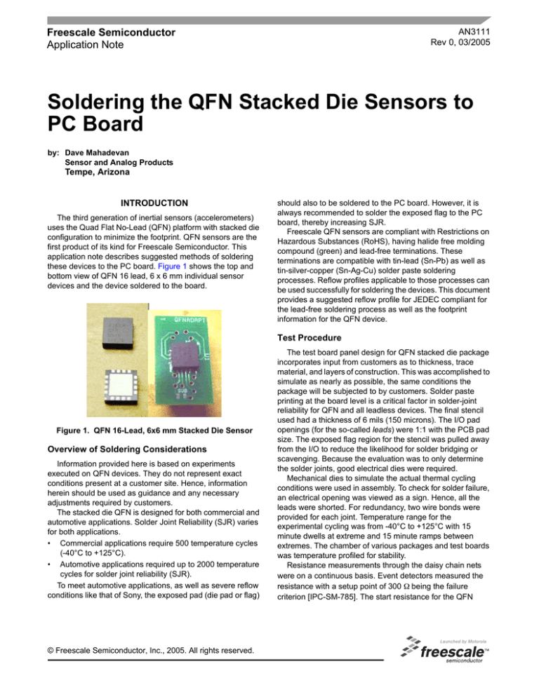
these devices to the PC board. Figure 1 shows the top and
bottom view of QFN 16 lead, 6 x 6 mm individual sensor
devices and the device soldered to the board.
should also to be soldered to the PC board. However, it is
always recommended to solder the exposed flag to the PC
board, thereby increasing SJR.
Freescale QFN sensors are compliant with Restrictions on
Hazardous Substances (RoHS), having halide free molding
compound (green) and lead-free terminations. These
terminations are compatible with tin-lead (Sn-Pb) as well as
tin-silver-copper (Sn-Ag-Cu) solder paste soldering
processes. Reflow profiles applicable to those processes can
be used successfully for soldering the devices. This document
provides a suggested reflow profile for JEDEC compliant for
the lead-free soldering process as well as the footprint
information for the QFN device.
Test Procedure
Figure 1. QFN 16-Lead, 6x6 mm Stacked Die Sensor
Overview of Soldering Considerations
Information provided here is based on experiments
executed on QFN devices. They do not represent exact
conditions present at a customer site. Hence, information
herein should be used as guidance and any necessary
adjustments required by customers.
The stacked die QFN is designed for both commercial and
automotive applications. Solder Joint Reliability (SJR) varies
for both applications.
• Commercial applications require 500 temperature cycles
(-40°C to +125°C).
• Automotive applications required up to 2000 temperature
cycles for solder joint reliability (SJR).
To meet automotive applications, as well as severe reflow
conditions like that of Sony, the exposed pad (die pad or flag)
© Freescale Semiconductor, Inc., 2005. All rights reserved.
The test board panel design for QFN stacked die package
incorporates input from customers as to thickness, trace
material, and layers of construction. This was accomplished to
simulate as nearly as possible, the same conditions the
package will be subjected to by customers. Solder paste
printing at the board level is a critical factor in solder-joint
reliability for QFN and all leadless devices. The final stencil
used had a thickness of 6 mils (150 microns). The I/O pad
openings (for the so-called leads) were 1:1 with the PCB pad
size. The exposed flag region for the stencil was pulled away
from the I/O to reduce the likelihood for solder bridging or
scavenging. Because the evaluation was to only determine
the solder joints, good electrical dies were required.
Mechanical dies to simulate the actual thermal cycling
conditions were used in assembly. To check for solder failure,
an electrical opening was viewed as a sign. Hence, all the
leads were shorted. For redundancy, two wire bonds were
provided for each joint. Temperature range for the
experimental cycling was from -40°C to +125°C with 15
minute dwells at extreme and 15 minute ramps between
extremes. The chamber of various packages and test boards
was temperature profiled for stability.
Resistance measurements through the daisy chain nets
were on a continuous basis. Event detectors measured the
resistance with a setup point of 300 Ω being the failure
criterion [IPC-SM-785]. The start resistance for the QFN
packages through the daisy chain was on the order of 1 Ω.
When the event detectors recorded a failure, the net failing
was identified and documented. Results indicated the first
failure (with exposed flags soldered down) was more than
2000 temperature cycles. The first failure, with Sony reflow
conditions, occurred beyond 1000 cycles with exposed flag
soldered down.
Figure 3 illustrates the footprint of the QFN 16 lead 6 x 6
mm package for solder paste printing purposes.
Summary
There are many new applications being designed using
QFN stacked die accelerometers. This document suggests
soldering methods for those devices.
Footprint and Reflow Profiles
Figure 2 provides the JEDEC compliant reflow conditions.
Target
30 sec. Large
20 sec. Small
Time Within 5°C of Peak
20 to 40 sec. Pb-Free, Small
10 to 30 sec. Pb-Free, Large
10 to 30 sec. SnPb
Temperature (°C)
250
Peak (Large / Small)
245°C/260°C Pb-Free
225°C / 245°C SnPb
3°C / sec. Maximum Ramp
183°C or 217°C to Peak
200
Target 75 sec.
150
90 to 180 sec.
150°C to 200°C
60 to 90 sec.
217°C Pb-Free
> 183°C SnPb
Target 130 sec.
100
3°C / sec. Maximum Ramp
50°C to 120°C
50
Thermal Couple on Package Body
Time and temperatures defined from JEDEC specifications with averages of approximately 30 customer inpute
0
25
50
75
100
125
150
175
200
225
250
Time (seconds)
Figure 2. Reflow Profile for Sn-Pb and Sn-Ag-CU Solder Paste Soldering Processes
6.0
0.55
4.25
12
9
13
8
6.0
1.00
0.50
5
16
1
4
Pin 1 ID (non metallic)
Solder Areas
Note: The die-pad (flag) should be soldered down for automotive use. All dimensions are in mm.
Figure 3. Footprint for 16-Lead OFN, 6 x 6 mm
AN3111
2
Sensor Device Data
Freescale Semiconductor
AN3111
Sensor Device Data
Freescale Semiconductor
3
How to Reach Us:
Home Page:
www.freescale.com
E-mail:
support@freescale.com
USA/Europe or Locations Not Listed:
Freescale Semiconductor
Technical Information Center, CH370
1300 N. Alma School Road
Chandler, Arizona 85224
+1-800-521-6274 or +1-480-768-2130
support@freescale.com
Europe, Middle East, and Africa:
Freescale Halbleiter Deutschland GmbH
Technical Information Center
Schatzbogen 7
81829 Muenchen, Germany
+44 1296 380 456 (English)
+46 8 52200080 (English)
+49 89 92103 559 (German)
+33 1 69 35 48 48 (French)
support@freescale.com
Japan:
Freescale Semiconductor Japan Ltd.
Headquarters
ARCO Tower 15F
1-8-1, Shimo-Meguro, Meguro-ku,
Tokyo 153-0064
Japan
0120 191014 or +81 3 5437 9125
support.japan@freescale.com
Asia/Pacific:
Freescale Semiconductor Hong Kong Ltd.
Technical Information Center
2 Dai King Street
Tai Po Industrial Estate
Tai Po, N.T., Hong Kong
+800 2666 8080
support.asia@freescale.com
For Literature Requests Only:
Freescale Semiconductor Literature Distribution Center
P.O. Box 5405
Denver, Colorado 80217
1-800-441-2447 or 303-675-2140
Fax: 303-675-2150
LDCForFreescaleSemiconductor@hibbertgroup.com
AN3111
Rev. 0
03/2005
Information in this document is provided solely to enable system and software
implementers to use Freescale Semiconductor products. There are no express or
implied copyright licenses granted hereunder to design or fabricate any integrated
circuits or integrated circuits based on the information in this document.
Freescale Semiconductor reserves the right to make changes without further notice to
any products herein. Freescale Semiconductor makes no warranty, representation or
guarantee regarding the suitability of its products for any particular purpose, nor does
Freescale Semiconductor assume any liability arising out of the application or use of any
product or circuit, and specifically disclaims any and all liability, including without
limitation consequential or incidental damages. “Typical” parameters that may be
provided in Freescale Semiconductor data sheets and/or specifications can and do vary
in different applications and actual performance may vary over time. All operating
parameters, including “Typicals”, must be validated for each customer application by
customer’s technical experts. Freescale Semiconductor does not convey any license
under its patent rights nor the rights of others. Freescale Semiconductor products are
not designed, intended, or authorized for use as components in systems intended for
surgical implant into the body, or other applications intended to support or sustain life,
or for any other application in which the failure of the Freescale Semiconductor product
could create a situation where personal injury or death may occur. Should Buyer
purchase or use Freescale Semiconductor products for any such unintended or
unauthorized application, Buyer shall indemnify and hold Freescale Semiconductor and
its officers, employees, subsidiaries, affiliates, and distributors harmless against all
claims, costs, damages, and expenses, and reasonable attorney fees arising out of,
directly or indirectly, any claim of personal injury or death associated with such
unintended or unauthorized use, even if such claim alleges that Freescale
Semiconductor was negligent regarding the design or manufacture of the part.
Freescale™ and the Freescale logo are trademarks of Freescale Semiconductor, Inc.
All other product or service names are the property of their respective owners.
© Freescale Semiconductor, Inc. 2005. All rights reserved.
