810251I
VCXO and Synchronous Ethernet
Jitter Attenuator
Data Sheet
General Description
Features
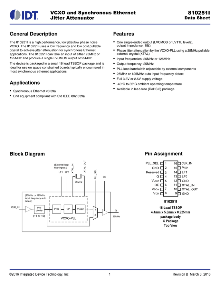
The 810251I is a high performance, low jitter/low phase noise
VCXO. The 810251i uses a low frequency and low cost pullable
crystal to achieve jitter attenuation for synchronous Ethernet
applications. The 810251I can take an input of either 25MHz or
125MHz and produce a single LVCMOS output of 25MHz.
•
One single-ended output (LVCMOS or LVTTL levels),
output Impedance: 15
•
Phase jitter attenuation by the VCXO-PLL using a 25MHz pullable
external crystal (XTAL)
•
•
•
•
•
•
•
Input frequencies: 25MHz or 125MHz
The device is packaged in a small 16 lead TSSOP package and is
ideal for use on space constrained boards typically encountered in
most synchronous ethernet applications.
Applications
•
•
Synchronous Ethernet v0.39a
Output frequency: 25MHz
PLL loop bandwidth adjustable by external components
25MHz or 125MHz auto input frequency detect
Full 3.3V or 2.5V supply voltage
-40°C to 85°C ambient operating temperature
Available in lead-free (RoHS 6) package
End equipment compliant with Std IEEE 802.039a
Pin Assignment
PLL_SEL
PLL_SEL
LF1 LF0
XTAL_IN
(External loop
filter inputs.)
XTAL_OUT
Block Diagram
GND
Reserved
Q
VDDO
OE
V DDA
V DD
OE
25MHz
(25MHz or 125MHz
input frequency auto
detect)
CLK_IN
Predivider
(÷1 or ÷5)
1
2
3
4
5
6
7
8
16
15
14
13
12
11
10
9
CLK_IN
V DD
LF1
LF0
GND
XTAL_IN
XTAL_OUT
GND
810251I
PFD
CP
VCXO
1
Q
0
25MHz
VCXO-PLL
©2016 Integrated Device Technology, Inc
1
16-Lead TSSOP
4.4mm x 5.0mm x 0.925mm
package body
G Package
Top View
Revision B March 3, 2016
810251I Data Sheet
Table 1. Pin Descriptions
Number
Name
Type
Description
Pullup
When logic HIGH, the VCXO-PLL is enabled. When LOW, the VCXO-PLL is in
bypass mode. LVCMOS/LVTTL interface levels.
1
PLL_SEL
Input
2, 9, 12
GND
Power
3
Reserved
Reserved
4
Q
Output
Single-ended clock output. LVCMOS/ LVTTL interface levels.
5
VDDO
Power
Output power supply pin.
6
OE
Input
Power supply ground.
Reserved pin. Do not connect.
Pullup
Output enable pin for Q output. LVCMOS/LVTTL interface levels.
7
VDDA
Power
Analog supply pin.
8, 15
VDD
Power
Core supply pins.
10,
11
XTAL_OUT,
XTAL_IN
Input
13, 14
LF0, LF1
Analog
Input/
Output
16
CLK_IN
Input
VCXO crystal oscillator interface. XTAL_IN is the input. XTAL_OUT is the output.
Loop filter connection node pins.
Pulldown
Single-ended clock input. LVCMOS/LVTTL interface levels.
NOTE: Pullup and Pulldown refer to internal input resistors. See Table 2, Pin Characteristics, for typical values.
Table 2. Pin Characteristics
Symbol
Parameter
CIN
Input Capacitance
CPD
Power Dissipation Capacitance
RPULLUP
Input Pullup Resistor
Test Conditions
Output Impedance
©2016 Integrated Device Technology, Inc
Typical
Maximum
Units
4
pF
VDD, VDDO = 3.465V
8
pF
VDD, VDDO = 2.625V
5
pF
51
k
51
k
VDDO = 3.3V±5%
15
VDDO = 2.5V±5%
20
RPULLDOWN Input Pulldown Resistor
ROUT
Minimum
2
Revision B March 3, 2016
810251I Data Sheet
Absolute Maximum Ratings
NOTE: Stresses beyond those listed under Absolute Maximum Ratings may cause permanent damage to the device.
These ratings are stress specifications only. Functional operation of product at these conditions or any conditions beyond
those listed in the DC Characteristics or AC Characteristics is not implied. Exposure to absolute maximum rating conditions for
extended periods may affect product reliability.
Item
Rating
Supply Voltage, VDD
4.6V
Inputs, VI
-0.5V to VDD + 0.5V
Outputs, VO
-0.5V to VDD + 0.5V
Package Thermal Impedance, JA
92.4C/W (0 mps)
Storage Temperature, TSTG
-65C to 150C
DC Electrical Characteristics
Table 3A. Power Supply DC Characteristics, VDD = VDDO = 3.3V ± 5%, TA = -40°C to 85°C
Symbol
Parameter
VDD
Core Supply Voltage
VDDA
Test Conditions
Minimum
Typical
Maximum
Units
3.135
3.3
3.465
V
Analog Supply Voltage
VDD – 0.07
3.3
VDD
V
VDDO
Output Supply Voltage
3.135
3.3
3.465
V
IDD
Power Supply Current
40
mA
IDDA
Analog Supply Current
7
mA
IDDO
Output Supply Current
5
mA
No Load
Table 3B. Power Supply DC Characteristics, VDD = VDDO = 2.5V ± 5%, TA = -40°C to 85°C
Symbol
Parameter
VDD
Core Supply Voltage
VDDA
Minimum
Typical
Maximum
Units
2.375
2.5
2.625
V
Analog Supply Voltage
VDD – 0.07
2.5
VDD
V
VDDO
Output Supply Voltage
2.375
2.5
2.625
V
IDD
Power Supply Current
35
mA
IDDA
Analog Supply Current
7
mA
IDDO
Output Supply Current
5
mA
©2016 Integrated Device Technology, Inc
Test Conditions
No Load
3
Revision B March 3, 2016
810251I Data Sheet
Table 3C. LVCMOS/LVTTL DC Characteristics, VDD = VDDO = 3.3V ± 5% or 2.5V ± 5%, TA = -40°C to 85°C
Symbol
Parameter
Test Conditions
Minimum
VDD = 3.465V
Typical
Maximum
Units
VIH
Input
High Voltage
2
VDD + 0.3
V
VDD = 2.625V
1.7
VDD + 0.3
V
VIL
Input
Low Voltage
VDD = 3.465V
-0.3
0.8
V
VDD = 2.625V
-0.3
0.7
V
Input
High Current
CLK_IN
IIH
VDD = VIN = 3.465V or 2.625V
150
µA
OE, PLL_SEL
VDD = VIN = 3.465V or 2.625V
5
µA
Input
Low Current
CLK_IN
VDD = 3.465V or 2.625V, VIN = 0V
-5
µA
IIL
OE, PLL_SEL
VDD = 3.465V or 2.625V, VIN = 0V
-150
µA
V
Output High Voltage; NOTE 1
VDDO = 3.3V ± 5%
2.6
VOH
VDDO = 2.5V ± 5%
1.8
V
VOL
Output Low Voltage; NOTE 1
VDDO = 3.3V ± 5%
0.6
V
VDDO = 2.5V ± 5%
0.5
V
NOTE 1: Outputs terminated with 50 to VDDO/2. See Parameter Measurement Information section. Load Test Circuit diagrams.
AC Electrical Characteristics
Table 4A. AC Characteristics, VDD = VDDO = 3.3V ± 5%, TA = -40°C to 85°C
Symbol
Parameter
Test Conditions
Minimum
Typical
125
MHz
MHz
Input Reference Frequency
fVCO
VCXO-PLL Frequency
25
fOUT
Output Frequency
25
tJIT(CC)
Cycle-to-Cycle Jitter; NOTE 1
tjit()
RMS Phase Jitter (Random);
NOTE 2
tJIT(PER)
Period jitter
Output Rise/Fall Time
odc
odc
MHz
45
fOUT = 25MHz, Integration Range:
1kHz – 1MHz
Units
MHz
fREF
tR / tF
Maximum
25
0.22
ps
ps
5
ps
500
1200
ps
Output Duty Cycle; NOTE 3
48
52
%
Output Duty Cycle; NOTE 4
45
55
%
20% to 80%
NOTE: Electrical parameters are guaranteed over the specified ambient operating temperature range, which is established when device is
mounted in a test socket with maintained transverse airflow greater than 500 lfpm. Device will meet specifications after thermal equilibrium has
been reached under these conditions.
NOTE: Characterized using a 616Hz bandwidth filter.
NOTE 1: This parameter is defined in accordance with JEDEC Standard 65.
NOTE 2: Please refer to the Phase Noise Plot.
NOTE 3: Specified with the VCXO-PLL free running high.
NOTE 4: Specified with the VCXO-PLL locked.
©2016 Integrated Device Technology, Inc
4
Revision B March 3, 2016
810251I Data Sheet
Table 4B. AC Characteristics, VDD = VDDO = 2.5V ± 5%, TA = -40°C to 85°C
Symbol
Parameter
fREF
Input Reference Frequency
fVCO
fOUT
Test Conditions
Minimum
Typical
Maximum
Units
25
MHz
125
MHz
VCXO-PLL Frequency
25
MHz
Output Frequency
25
MHz
tJIT(CC)
Cycle-to-Cycle Jitter; NOTE 1
tjit
RMS Phase Jitter (Random);
NOTE 2
tJIT(PER)
Period jitter
35
fOUT = 25MHz, Integration Range:
1kHz – 1MHz
20% to 80%
0.24
ps
ps
10
ps
tR / tF
Output Rise/Fall Time
700
2200
ps
odc
Output Duty Cycle; NOTE 3
48
52
%
odc
Output Duty Cycle; NOTE 4
44
56
%
NOTE: Electrical parameters are guaranteed over the specified ambient operating temperature range, which is established when device is
mounted in a test socket with maintained transverse airflow greater than 500 lfpm. Device will meet specifications after thermal equilibrium has
been reached under these conditions.
NOTE: Characterized using a 616Hz bandwidth filter.
NOTE 1: This parameter is defined in accordance with JEDEC Standard 65.
NOTE 2: Please refer to the Phase Noise Plot.
NOTE 3: Specified with the VCXO-PLL free running high.
NOTE 4: Specified with the VCXO-PLL locked.
©2016 Integrated Device Technology, Inc
5
Revision B March 3, 2016
810251I Data Sheet
➝
Typical Phase Noise at 25MHz (3.3V)
Ethernet Filter
Noise Power dBc
Hz
25MHz
RMS Phase Jitter (Random)
1kHz to 1MHz = 0.22ps (typical)
➝
➝
Raw Phase Noise Data
Phase Noise Result by adding
an Ethernet filter to raw data
Offset Frequency (Hz)
➝
Typical Phase Noise at 25MHz (2.5V)
Ethernet Filter
Noise Power dBc
Hz
25MHz
RMS Phase Jitter (Random)
1kHz to 1MHz = 0.24ps (typical)
➝
➝
Raw Phase Noise Data
Phase Noise Result by adding
an Ethernet filter to raw data
Offset Frequency (Hz)
©2016 Integrated Device Technology, Inc
6
Revision B March 3, 2016
810251I Data Sheet
Parameter Measurement Information
1.25V±5
1.65V±5
1.65V±5
1.25V±5
SCOPE
VDD,
VDDA
SCOPE
VDD,
VDDO
VDDO
VDDA
Qx
GND
Qx
GND
-1.65V±5
-1.25V±5
3.3V Core/3.3V LVCMOS Output Load AC Test Circuit
2.5V Core/2.5V LVCMOS Output Load AC Test Circuit
Phase Noise Plot
V
DDO
V
DDO
2
DDO
2
➤
tcycle n
➤
Noise Power
V
Q
2
tcycle n+1
➤
Phase Noise Mask
➤
tjit(cc) = |tcycle n – tcycle n+1|
1000 Cycles
f1
Offset Frequency
f2
RMS Jitter = Area Under the Masked Phase Noise Plot
Cycle-to-Cycle Jitter
RMS Phase Jitter
VOH
VREF
80%
1σ contains 68.26% of all measurements
2σ contains 95.4% of all measurements
3σ contains 99.73% of all measurements
4σ contains 99.99366% of all measurements
6σ contains (100-1.973x10⁻⁷)% of all measurements
Reference Point
(Trigger Edge)
80%
VOL
20%
20%
Q
tR
tF
Histogram
Mean Period
(First edge after trigger)
Period Jitter
©2016 Integrated Device Technology, Inc
Output Rise/Fall Time
7
Revision B March 3, 2016
810251I Data Sheet
Parameter Measurement Information, continued
V
DDO
2
Q
t PW
t
odc =
PERIOD
t PW
x 100%
t PERIOD
Output Duty Cycle/Pulse Width/Period
Application Information
Recommendations for Unused Input Pins
Inputs:
LVCMOS Control Pins
All control pins have internal pull-ups or pull-downs; additional
resistance is not required but can be added for additional protection.
A 1k resistor can be used.
©2016 Integrated Device Technology, Inc
8
Revision B March 3, 2016
810251I Data Sheet
Schematic Example
3-pole filter can also be used for additional spur reduction. It is
recommended that the loop filter components be laid out for the
3-pole option. This will also allow the 2-pole filter to be used.
Figure 1 shows an example of the 810251I application schematic. In
this example, the device is operated either at VDD = 3.3V or 2.5V.
The decoupling capacitors should be located as close as possible to
the power pin. The input is driven by an LVCMOS driver. An optional
3-pole loop filter example - (optional)
R3
LF0
LF1
Rs
TBD
VDD
TBD
VDDO
Cp
TBD
Cs
TBD
C3
TBD
C1
0.1u
C2
0.1u
VDD
XTAL_OUT
XTAL_IN
C5
SPARE
X2
Rs
1K
C6
SPARE
9
10
11
12
13
14
15
16
GND
XTAL_OUT
XTAL_IN
GND
LF0
LF1
VDD
CLK_IN
VDD
VDDA
OE
VDDO
Q
Reserv ed
GND
PLL_SEL
R2
8
7
6
5
4
3
2
1
VDDA
C30
0.01u
Cp
0.001 uF
Cs
10uF
R4
Logic Control Input Examples
Q1
R1
Set Logic
Input to
'1'
VDD
33
Zo = 50
C45
10u
Zo = 50
C4
U1
0.1u
2-pole loop filter
VDD
10
RU1
1K
LVCMOS_Driv er
LVCMOS_Receiv er
Set Logic
Input to
'0'
VDD
RU2
Not Install
To Logic
Input
pins
RD1
Not Install
33
VDD=VDDO=3.3V
To Logic
Input
pins
RD2
1K
Figure 1. P.C. 810251I Schematic Example
©2016 Integrated Device Technology, Inc
9
Revision B March 3, 2016
810251I Data Sheet
VCXO-PLL EXTERNAL COMPONENTS
Choosing the correct external components and having a proper
printed circuit board (PCB) layout is a key task for quality operation
of the VCXO-PLL. In choosing a crystal, special precaution must be
taken with the package and load capacitance (CL). In addition,
frequency, accuracy and temperature range must also be
considered. Since the pulling range of a crystal also varies with the
package, it is recommended that a metal-canned package like HC49
be used. Generally, a metal-canned package has a larger pulling
range than a surface mounted device (SMD). For crystal selection
information, refer to the VCXO Crystal Selection Application Note.
The frequency of oscillation in the third overtone mode is not
necessarily at exactly three times the fundamental frequency. The
mechanical properties of the quartz element dictate the position of
the overtones relative to the fundamental. The oscillator circuit may
excite both the fundamental and overtone modes simultaneously.
This will cause a nonlinearity in the tuning curve. This potential
problem is why VCXO crystals are required to be tested for absence
of any activity inside a +/-200 ppm window at three times the
fundamental frequency. Refer to FL_3OVT and FL_3OVT_spurs in the
crystal Characteristics table.
The crystal’s load capacitance CL characteristic determines its
resonating frequency and is closely related to the VCXO tuning
range. The total external capacitance seen by the crystal when
installed on a board is the sum of the stray board capacitance, IC
package lead capacitance, internal varactor capacitance and any
installed tuning capacitors (CTUNE).
The crystal and external loop filter
components should be kept as
close as possible to the device.
Loop filter and crystal traces
should be kept short and
separated from each other. Other
signal traces should be kept
separate and not run underneath
the device, loop filter or crystal
components.
If the crystal CL is greater than the total external capacitance, the
VCXO will oscillate at a higher frequency than the crystal
specification. If the crystal CL is lower than the total external
capacitance, the VCXO will oscillate at a lower frequency than the
crystal specification. In either case, the absolute tuning range is
reduced. The correct value of CL is dependant on the characteristics
of the VCXO. The recommended CL in the Crystal Parameter Table
balances the tuning range by centering the tuning curve.
LF0
LF1
RS
CP
CS
XTAL_IN
CTUNE
25MHz
XTAL_OUT
CTUNE
VCXO Characteristics Table
Symbol
Parameter
Typical
Units
kVCXO
VCXO Gain
15000
Hz/V
CV_LOW
Low Varactor Capacitance
9.8
pF
CV_HIGH
High Varactor Capacitance
22.7
pF
VCXO-PLL Loop Bandwidth Selection Table
Bandwidth
Crystal Frequency (MHz)
RS (k)
CS (µF)
CP (µF)
246Hz (Low)
25
0.4
10
0.01
616Hz (Mid)
25
1.0
10
0.001
1000Hz (High)
25
1.65
10
0.001
Crystal Characteristics
Symbol
Parameter
Test Conditions
Minimum
Mode of Oscillation
Typical
Maximum
Units
Fundamental
fN
Frequency
25
fT
Frequency Tolerance
±20
ppm
fS
Frequency Stability
±20
ppm
+85
0C
Operating Temperature Range
-40
MHz
CL
Load Capacitance
CO
Shunt Capacitance
CO / C1
Pullability Ratio
ESR
Equivalent Series Resistance
20
Drive Level
1
mW
±3 per year
ppm
Aging @ 25
10
4
220
0C
©2016 Integrated Device Technology, Inc
pF
10
pF
240
Revision B March 3, 2016
810251I Data Sheet
Power Considerations
This section provides information on power dissipation and junction temperature for the 810251I.
Equations and example calculations are also provided.
1.
Power Dissipation.
The total power dissipation for the 810251I is the sum of the core power plus the analog power plus the power dissipated in the load(s). The
following is the power dissipation for VDD = 3.3V + 5% = 3.465V, which gives worst case results.
•
Power (core)MAX = VDD_MAX * (IDD + IDDA + IDDO) = 3.465V *(40mA + 7mA + 5mA) = 180.18mW
•
Output Impedance ROUT Power Dissipation due to Loading 50 to VDD/2
Output Current IOUT = VDD_MAX / [2 * (50 + ROUT)] = 3.465V / [2 * (50 + 15)] = 26.7mA
•
Power Dissipation on the ROUT per LVCMOS output
Power (ROUT) = ROUT * (IOUT)2 = 15 * (26.7mA)2 = 10.7mW per output
Dynamic Power Dissipation at 25MHz
Power (25MHz) = CPD * Frequency * (VDD)2 = 8pF * 25MHz * (3.465V)2 = 2.4mW per output
Total Power Dissipation
•
Total Power
= Power (core)MAX + Power (ROUT) + Power (25MHz)
= 180.18mW + 10.7mW + 2.4mW
= 193.28mW
2. Junction Temperature.
Junction temperature, Tj, is the temperature at the junction of the bond wire and bond pad and it directly affects the reliability of the device. The
maximum recommended junction temperature is 125°C. Limiting the internal transistor junction temperature, Tj, to 125°C ensures that the bond
wire and bond pad temperature remains below 125°C.
The equation for Tj is as follows: Tj = JA * Pd_total + TA
Tj = Junction Temperature
JA = Junction-to-Ambient Thermal Resistance
Pd_total = Total Device Power Dissipation (example calculation is in section 1 above)
TA = Ambient Temperature
In order to calculate junction temperature, the appropriate junction-to-ambient thermal resistance JA must be used. Assuming no air flow and
a multi-layer board, the appropriate value is 92.4°C/W per Table 5 below.
Therefore, Tj for an ambient temperature of 85°C with all outputs switching is:
85°C + 0.193W *92.4°C/W = 102.8°C. This is well below the limit of 125°C.
This calculation is only an example. Tj will obviously vary depending on the number of loaded outputs, supply voltage, air flow and the type of
board (multi-layer).
Table 5. Thermal Resistance JA for 16 Lead TSSOP, Forced Convection
JA by Velocity
Meters per Second
Multi-Layer PCB, JEDEC Standard Test Boards
©2016 Integrated Device Technology, Inc
0
1
2.5
92.4°C/W
88.0°C/W
85.9°C/W
11
Revision B March 3, 2016
810251I Data Sheet
Reliability Information
Table 6. JA vs. Air Flow Table for a 16 Lead TSSOP
JA vs. Air Flow
Meters per Second
Multi-Layer PCB, JEDEC Standard Test Boards
0
1
2.5
92.4°C/W
88.0°C/W
85.9°C/W
Transistor Count
The transistor count for 810251I: 937
Package Outline and Package Dimensions
Package Outline - G Suffix for 16 Lead TSSOP
Table 7. Package Dimensions for 16 Lead TSSOP
All Dimensions in Millimeters
Symbol
Minimum
Maximum
N
16
A
1.20
A1
0.5
0.15
A2
0.80
1.05
b
0.19
0.30
c
0.09
0.20
D
4.90
5.10
E
6.40 Basic
E1
4.30
4.50
e
0.65 Basic
L
0.45
0.75
0°
8°
aaa
0.10
Reference Document: JEDEC Publication 95, MO-153
©2016 Integrated Device Technology, Inc
12
Revision B March 3, 2016
810251I Data Sheet
Ordering Information
Table 8. Ordering Information
Part/Order Number
810251AGILF
810251AGILFT
Marking
10251AIL
10251AIL
©2016 Integrated Device Technology, Inc
Package
16 Lead “Lead-Free” TSSOP
16 Lead “Lead-Free” TSSOP
13
Shipping Packaging
Tube
Tape & Reel
Temperature
-40C to 85C
-40C to 85C
Revision B March 3, 2016
810251I Data Sheet
Revision History Sheet
Rev
Table
Page
1
10
A
B
B
B
T8
14
T4A
1
4
T4B
5
T4A
T4B
T8
4
5
13
Description of Change
Date
Updated Figure 1, Schematic layout.
VCXO-PLL External Components section, reworded second from last paragraph
“The frequency of oscillation in the third overtone mode....”.
Changed marking from 810251AL to 10251AL.
Changed datasheet header/footer format.
7/28/09
Features List: deleted ‘Absolute pull range is ±50 ppm (using the internal oscillator)’
3.3V AC Characteristics Table - Added additional odc row with specs of 45min and 55max.
Added Notes 3 & 4.
2.5V AC Characteristics Table - Added additional odc row with specs of 44min and 56max.
Added Notes 3 & 4.
HiPerClock references have been deleted throughout the datasheet.
7/17/2012
Added ‘high’ to Note 3.
Added ‘high’ to Note 3.
Deleted quantity from Tape and Reel.
10/5/2012
Removed ICS from the part number where needed.
Updated data sheet header and footer.
©2016 Integrated Device Technology, Inc
14
3/3/16
Revision B March 3, 2016
810251I Data Sheet
Corporate Headquarters
Sales
Tech Support
6024 Silver Creek Valley Road
San Jose, CA 95138 USA
www.IDT.com
1-800-345-7015 or 408-284-8200
Fax: 408-284-2775
www.IDT.com/go/sales
www.idt.com/go/support
DISCLAIMER Integrated Device Technology, Inc. (IDT) reserves the right to modify the products and/or specifications described herein at any time, without notice, at IDT's sole discretion. Performance specifications
and operating parameters of the described products are determined in an independent state and are not guaranteed to perform the same way when installed in customer products. The information contained herein
is provided without representation or warranty of any kind, whether express or implied, including, but not limited to, the suitability of IDT's products for any particular purpose, an implied warranty of merchantability,
or non-infringement of the intellectual property rights of others. This document is presented only as a guide and does not convey any license under intellectual property rights of IDT or any third parties.
IDT's products are not intended for use in applications involving extreme environmental conditions or in life support systems or similar devices where the failure or malfunction of an IDT product can be reasonably
expected to significantly affect the health or safety of users. Anyone using an IDT product in such a manner does so at their own risk, absent an express, written agreement by IDT.
Integrated Device Technology, IDT and the IDT logo are trademarks or registered trademarks of IDT and its subsidiaries in the United States and other countries. Other trademarks used herein are the property of
IDT or their respective third party owners.
For datasheet type definitions and a glossary of common terms, visit www.idt.com/go/glossary.
Copyright ©2016 Integrated Device Technology, Inc. All rights reserved.


