MP2127
2.7-6V Input, 2A, 1.2MHz
Synchronous Step-Down Converter
The Future of Analog IC Technology
DESCRIPTION
FEATURES
The MP2127 is a fully integrated, internally
compensated 1.2MHz fixed frequency PWM
step-down converter. It is ideal for powering
portable equipment that runs from a single cell
Lithium-Ion (Li+) Battery, with an input range
from 2.7V to 6V. The MP2127 can provide up to
2A of load current with output voltage as low as
0.8V. It can also operate at 100% duty cycle for
low dropout applications. With peak current
mode control and internal compensation, the
MP2127 is stable with ceramic capacitors and
small inductors. Fault condition protection
includes cycle-by-cycle current limiting and
thermal shutdown.
•
•
•
MP2127 is available in
3mmx3mm QFN package.
the
small
6-pin
•
•
•
•
•
•
•
•
Output Adjustable from 0.8V to VIN
Up to 95% Efficiency
100% Duty Cycle for Low Dropout
Applications
Power Good Indicator Output
1.2MHz Fixed Switching Frequency
Stable with Low ESR Output Ceramic
Capacitors
Thermal Shutdown
Cycle-by-Cycle Over Current Protection
Short circuit protection
2.7V-6V Input Operation Range
Available in 6-pin 3x3mm QFN
APPLICATIONS
•
•
•
•
Smart Phones, PDA’s
DVD+/-RW Drives
Digital Cameras
Portable Instruments
“MPS” and “The Future of Analog IC Technology” are Trademarks of Monolithic
Power Systems, Inc.
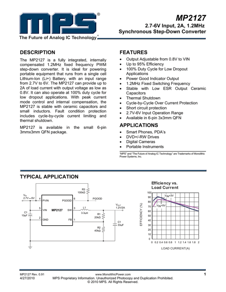
TYPICAL APPLICATION
R3
100k
6V
4
5
C1
10
2
PVIN
VIN
GND
PGOOD
MP2127
SW
VOUT
1.2V/2A
L1
3.3
FB 1
90
PGOOD
6
3
100
R1
20k
R2
40k
C1
33
EFFICIENCY (%)
VIN
2.7V
Efficiency vs.
Load Current
VIN=3V
80
70
VIN=5V
60
50
40
30
20
10
0
0 0.2 0.4 0.6 0.8 1 1.2 1.4 1.6 1.8 2
LOAD CURRENT(A)
MP2127 Rev. 0.91
4/27/2010
www.MonolithicPower.com
MPS Proprietary Information. Unauthorized Photocopy and Duplication Prohibited.
© 2010 MPS. All Rights Reserved.
1
MP2127 – 2.7-6V, 2A, 1.2MHZ SYNCHRONOUS STEP-DOWN CONVERTER
ORDERING INFORMATION
Part Number*
MP2127DQ
Package
QFN6 (3mm x 3mm)
Top Marking
Free Air Temperature (TA)
8G
–40°C to +85°C
* For Tape & Reel, add suffix –Z (e.g. MP2127DQ–Z).
For RoHS compliant packaging, add suffix –LF (e.g. MP2127DQ–LF–Z)
PACKAGE REFERENCE
TOP VIEW
FB
1
6
PGOOD
GND
2
5
VIN
SW
3
4
PVIN
ABSOLUTE MAXIMUM RATINGS (1)
Recommended Operating Conditions
PVIN, VIN to GND......................–0.3V to + 7.0V
SW to GND .......................... –0.3V to VIN + 0.3V
PGOOD, FB to GND ...................–0.3V to +6.5V
Operating Temperature............. –40°C to +85°C
Continuous Power Dissipation…(TA = +25°C) (2)
………………………………………………....2.5W
Junction Temperature ...............................150°C
Lead Temperature ....................................260°C
Storage Temperature ............. –65°C to +150°C
Supply Voltage VIN .............................2.7V to 6V
Operating Junct. Temp (TJ)...... -40°C to +125°C
MP2127 Rev. 0.91
4/27/2010
Thermal Resistance
(4)
θJA
(3)
θJC
QFN6 (3mm x 3mm) ...............50 ...... 12 ... °C/W
Notes:
1) Exceeding these ratings may damage the device.
2) The maximum allowable power dissipation is a function of the
maximum junction temperature TJ (MAX), the junction-toambient thermal resistance θJA, and the ambient temperature
TA. The maximum allowable continuous power dissipation at
any ambient temperature is calculated by PD (MAX) = (TJ
(MAX)-TA)/θJA. Exceeding the maximum allowable power
dissipation will cause excessive die temperature, and the
regulator will go into thermal shutdown. Internal thermal
shutdown circuitry protects the device from permanent
damage.
3) The device is not guaranteed to function outside of its
operating conditions.
4) Measured on JESD51-7, 4-layer PCB.
www.MonolithicPower.com
MPS Proprietary Information. Unauthorized Photocopy and Duplication Prohibited.
© 2010 MPS. All Rights Reserved.
2
MP2127 – 2.7-6V, 2A, 1.2MHZ SYNCHRONOUS STEP-DOWN CONVERTER
ELECTRICAL CHARACTERISTICS (5)
VIN = 3.6V, TA = +25°C, unless otherwise noted.
Parameters
Supply Current
Thermal
Shutdown
Trip
Threshold
IN Undervoltage Lockout
Threshold
IN Undervoltage Lockout
Hysteresis
Regulated FB Voltage
FB Input Bias Current
SW PFET On Resistance
SW NFET On Resistance
SW PFET Peak Current
Limit
Switching Frequency
OVP threshold (PGOOD
Output High)
OVP
threshold
(Fault
Detected)
OVP Hysteresis
Symbol
Condition
IIN
TSD
INUVVTH
Typ
Max
Units
VFB = 0.9V
500
750
μA
Hysteresis = 20°C
150
Rising Edge
2.15
INUVHYS
VFB
IFB
HSRDS-ON
LSRDS-ON
ILIMIT
VFB OVPVFB OVP+
2.40
°C
2.65
160
TA = +25°C
-40°C≤ TA≤ +85°C
VFB = 0.9V
ISW = 100mA
ISW = -100mA
Duty Cycle=100%
Duty Cycle=50% (6)
0.784
0.776
-50
0.19
0.16
2.2
2.5
1.0
FSW
VFB ramps up from
nominal operating point
VFB ramps up from
nominal operating point
VFB
0.800
0.800
-2
0.23
0.2
3.0
3.5
1.2
0.816
0.824
+50
0.27
0.24
3.8
4.5
1.4
103%
VFB OVP+
PGOOD, Output Low
VFB OVP-
4.5V≤VIN≤5.5V, IOUT=100mA
0A ≤IOUT≤ 2A
V
nA
Ω
Ω
A
MHz
VFB
VFB
Ramp up VFB, starting at
VFB≤700mV
Ramp down VFB,starting at
VFB= VFB nom
ISINK = 6mA
V
mV
111%
25
PGOOD, Output High
PGOOD output low voltage
PGOOD Deglitch Time
Line Regulation
Load Regulation
Min
94%
160
0.1
0.1
VFB
mV
98.5%
VFB
95%
VFB
0.4
V
μs
%
%
Notes:
5) Production test at +25°C. Specifications over the temperature range are guaranteed by design and characterization.
6) Guaranteed by design
MP2127 Rev. 0.91
4/27/2010
www.MonolithicPower.com
MPS Proprietary Information. Unauthorized Photocopy and Duplication Prohibited.
© 2010 MPS. All Rights Reserved.
3
MP2127 – 2.7-6V, 2A, 1.2MHZ SYNCHRONOUS STEP-DOWN CONVERTER
PIN FUNCTIONS
Pin #
Name
1
FB
2
GND
3
4
5
SW
PVIN
VIN
6
PGOOD
MP2127 Rev. 0.91
4/27/2010
Description
Feedback input. An external resistor divider from the output to GND, tapped to the FB pin
sets the output voltage.
Ground pin. This pin is the reference ground of the regulated output voltage. For this
reason care must be taken in PCB layout. Suggested to be connected to GND with copper
and vias. Connect exposed pad to ground plane for proper thermal performance.
Switch node to the inductor
Input supply pin for power FET
Input Supply pin for controller
Power-good indicator output. “Low” output indicates output is outside the window of
regulation level. PGOOD is pulled down in shutdown. PGOOD output has 160us deglitch
timer to avoid false trigger during transient response.
www.MonolithicPower.com
MPS Proprietary Information. Unauthorized Photocopy and Duplication Prohibited.
© 2010 MPS. All Rights Reserved.
4
MP2127 – 2.7-6V, 2A, 1.2MHZ SYNCHRONOUS STEP-DOWN CONVERTER
TYPICAL PERFORMANCE CHARACTERISTICS
VIN = 5V, VOUT = 1.2V, TA = +25ºC, unless otherwise noted.
VIN=3V
660
640
VIN=5V
620
60
IIN (uA)
50
40
600
580
560
30
20
540
10
520
500
0
0
0 0.2 0.4 0.6 0.8 1 1.2 1.4 1.6 1.8 2
2
4
0.20
VIN=5V
0.12
0.08
0.04
VIN=3V
-0.04
-0.08
-0.12
-0.16
-0.20
0
0.5
1
1.5
LOAD CURRENT(A)
MP2127 Rev. 0.91
4/27/2010
35
30
25
20
15
10
5
0
0
8
2
0.5
1
1.5
2
OUTPUT CURRENT (A)
Line Regulation
NORMALIZED OUTPUT VOLTAGE (%)
NORMALIZED OUTPUT VOLTAGE (%)
Load Regulation
0.00
40
V IN(V)
LOAD CURRENT(A)
0.16
6
Ipeak vs. Duty
4.2
0.20
IO=0A
0.15
3.9
0.10
0.05
IPEAK (A)
EFFICIENCY (%)
80
70
CASE TEMPERATURE RISE (OC)
680
100
90
Case Tem perature Rise
vs. Output Current
Enabled Supply Current
vs. Input Voltage
Efficiency vs. Load Current
IO=1A
0.00
-0.05
-0.10
3.6
3.3
IO=2A
-0.15
3
-0.20
2
3
4
5
6
INPUT VOLTAGE (V)
7
0%
20%
40%
60%
80% 100%
DUTY CYCLE
www.MonolithicPower.com
MPS Proprietary Information. Unauthorized Photocopy and Duplication Prohibited.
© 2010 MPS. All Rights Reserved.
5
MP2127 – 2.7-6V, 2A, 1.2MHZ SYNCHRONOUS STEP-DOWN CONVERTER
TYPICAL PERFORMANCE CHARACTERISTICS (continued)
VIN = 5V, VOUT = 1.2V, TA = +25ºC, unless otherwise noted.
Short Entry
Short Recovery
Full Load
Full Load
VOUT
1V/div
VOUT
500mV/div
VOUT
500mV/div
SW
2V/div
SW
5V/div
SW
2V/div
VIN
5V/div
IINDUCTOR
2A/div
VIN
5V/div
IINDUCTOR
2A/div
IINDUCTOR
2A/div
SW
5V/div
VIN
5V/div
IINDUCTOR
2A/div
Power Good
Power Good
Power Up with 2A Load
VOUT
500mV/div
Power Up without Load
VOUT
1V/div
VOUT
1V/div
SW
5V/div
SW
5V/div
PGood
5V/div
PGood
5V/div
IINDUCTOR
500mA/div
IINDUCTOR
500mA/div
Input Ripple Voltage
Output Ripple Voltage
Load Transient Response
Full Load
IOUT=2A
IOUT=1A-2A
VOUT
20mV/div
VIN
50mV/div
VOUT
50mV/div
SW
2V/div
VIN
5V/div
SW
2V/div
400ns/div
MP2127 Rev. 0.91
4/27/2010
IINDUCTOR
2A/div
400ns/div
IOUT
1A/div
www.MonolithicPower.com
MPS Proprietary Information. Unauthorized Photocopy and Duplication Prohibited.
© 2010 MPS. All Rights Reserved.
6
MP2127 – 2.7-6V, 2A, 1.2MHZ SYNCHRONOUS STEP-DOWN CONVERTER
FUNCTIONAL BLOCK DIAGRAM
PVIN
VIN
Bias
&
Voltage
Reference
0.8V
ICS
Slope Comp
+
RI
IAMP
10X
Current
Sense Amp
0.74V
Feedback
Error Amp
EAO
EAMP
FB
To controller
blocks
0.86V
-
0.04
-
Main
Switch
(PCH)
+
+
+
PWMCMP
PWM
PWM
240k
RZ
CC
1.1M
17pF
SW
Control
1.2MHz
Oscillator
OSC
Logic
Synchronou
s Rectifier
(NCH)
GND
0.86V
+
COMP
PGOOD
+
COMP
0.74V
MP2127 Rev. 0.91
4/27/2010
-
www.MonolithicPower.com
MPS Proprietary Information. Unauthorized Photocopy and Duplication Prohibited.
© 2010 MPS. All Rights Reserved.
7
MP2127 – 2.7-6V, 2A, 1.2MHZ SYNCHRONOUS STEP-DOWN CONVERTER
OPERATION
The MP2127 is a fixed frequency 1.2MHz current
mode 2A step-down converter, optimized for low
voltage, Li-Ion battery powered applications
where high efficiency and small size are critical.
MP2127 integrates a high side PFET main switch
and a low side synchronous rectifier. It always
operates in continuous conduction mode,
simplifies the control scheme and eliminates the
random spectrum noise due to discontinuous
conduction mode.
The steady state duty cycle D for this mode can
be calculated as:
D = TON × fOSC × 100% ≈
VOUT
× 100%
VIN
Where TON is the main switch on time and fOSC is
the oscillator frequency (1.2MHz typ.).
Current Mode PWM Control
Slope compensated current mode PWM control
provides stable switching and cycle-by-cycle
current limiting for superior load and line
response as well as protection of the internal
main switch and synchronous rectifier. The
MP2127 switches at a constant frequency
(1.2MHz) and modulates the inductor peak
current to regulate the output voltage. Specifically,
for each cycle the PWM controller forces the
inductor peak current to an internal reference
level derived from the feedback error voltage. At
normal operation, the main switch is turned on at
each rise edge of the internal oscillator, and
remains on for a certain period of time to ramp up
the inductor current. As soon as the inductor
current reaches the reference level, the main
switch is turned off and immediately the
synchronous rectifier will be turned on to provide
the inductor current. In forced PWM mode, the
synchronous rectifier will stay on until the next
oscillator cycle.
MP2127 Rev. 0.91
4/27/2010
Dropout Operation
The MP2127 allows the main switch to remain on
for more than one switching cycle to increase the
duty cycle when the input voltage is dropping
close to the output voltage. When the duty cycle
reaches 100%, the main switch is held on
continuously to deliver current to the output up to
the PFET current limit. In this case, the output
voltage becomes the input voltage minus the
voltage drop across the main switch and the
inductor.
Maximum Load Current
The MP2127 can operate down to 2.7V input
voltage; however the maximum load current
decreases at lower input due to a large IR drop
on the main switch and synchronous rectifier.
The slope compensation signal reduces the peak
inductor current as a function of the duty cycle to
prevent sub-harmonic oscillations at duty cycles
greater than 50%. Conversely, the current limit
increases as the duty cycle decreases.
Short Circuit Protection
When the output is shorted to ground, the
oscillator frequency is reduced to prevent the
inductor current from increasing beyond the
PFET current limit. The PFET current limit is also
reduced to lower the short circuit current. The
frequency and current limit will return to the
normal values once the short circuit condition is
removed and the feedback voltage approaches
0.8V.
PGOOD Indicator
MP2127 provides an open-drain PGOOD output
that becomes high-impedance (open circuit) after
output level reaches regulation after startup.
PGOOD is pulled low if the output goes out of
regulation level for more than the de-glitch time
of 160us, or when device enters shutdown.
www.MonolithicPower.com
MPS Proprietary Information. Unauthorized Photocopy and Duplication Prohibited.
© 2010 MPS. All Rights Reserved.
8
MP2127 – 2.7-6V, 2A, 1.2MHZ SYNCHRONOUS STEP-DOWN CONVERTER
APPLICATION INFORMATION
Output Voltage Setting
The output voltage is set by the external resistor
divider:
VOUT = 0.8 ⋅ (1 +
R1
)
R2
1
R1 + 240k ⋅ (1 +
R1
)
R2
To minimize the impact of R1 to loop bandwidth,
one should choose R1 much smaller than 240k.
Some recommended value for common output
voltage is listed below:
Table 1—Resistor Selection vs. Output
Voltage Setting
VOUT
R1
1.2V
1.8V
2.5V
R2
20kΩ (1%) 40.2kΩ (1%)
49.9kΩ (1%) 40.2kΩ (1%)
84.5kΩ (1%) 40.2kΩ (1%)
Inductor Selection
A 1μH to 10μH inductor with DC current rating at
least 25% higher than the maximum load current
is recommended for most applications. For best
efficiency, the inductor DC resistance shall be
<200mΩ. See Table 2 for recommended
inductors and manufacturers. For most designs,
the inductance value can be derived from the
following equation:
L=
VOUT × (VIN − VOUT )
VIN × ΔIL × fOSC
Where ΔIL is inductor ripple current. Choose
inductor ripple current approximately 30% of the
maximum load current, 2A.
The maximum inductor peak current is:
IL(MAX ) = ILOAD +
MP2127 Rev. 0.91
4/27/2010
Manufacturer Part Number
TOKO
The divider ratio also affects the loop bandwidth of
the step-down converter. The approximate
relationship between them is given below:
BW ∝
Table 2—Suggested Inductors
TDK
B1015AS3R0N
RLF7030T3R3M4R1
Inductance
(μH)
Dimensions
LxWxH
(mm3)
3
8.4X8.3X4
3.3
7.3X6.8X3.2
Input Capacitor CIN Selection
The input capacitor reduces the surge current
drawn from the input and switching noise from
the device. The input capacitor impedance at the
switching frequency shall be less than input
source impedance to prevent high frequency
switching current passing to the input
Ceramic capacitors with X5R or X7R dielectrics
are highly recommended because of their low
ESR and small temperature coefficients. For
most applications, a 10μF capacitor is sufficient.
Output Capacitor COUT Selection
The output capacitor keeps output voltage ripple
small and ensures regulation loop stable. The
output capacitor impedance shall be low at the
switching frequency. Ceramic capacitors with
X5R or X7R dielectrics are recommended. For
forced PWM mode operation, the output ripple
ΔVOUT is approximately:
V
⋅ (V IN − VOUT )
1
1
ΔVOUT = OUT
( R ESR + ⋅
)F
V IN ⋅ f OSC ⋅ L
8 f OSC ⋅ C OUT
or most applications, a 33μF capacitor is
sufficient.
Thermal Dissipation
Power dissipation shall be considered when
operates MP2127 at maximum 2A output current.
If the junction temperature rises above 150°C,
MP2127 will be shut down by internal thermal
protection circuitry.
ΔIL
2
www.MonolithicPower.com
MPS Proprietary Information. Unauthorized Photocopy and Duplication Prohibited.
© 2010 MPS. All Rights Reserved.
9
MP2127 – 2.7-6V, 2A, 1.2MHZ SYNCHRONOUS STEP-DOWN CONVERTER
The junction-to-ambient thermal resistance of the
6-pin QFN (3mm x 3mm) RΘJA is 50°C/W. The
maximum allowable power dissipation is
about1.6W when MP2127 is operating in a 70°C
ambient temperature environment:
150 o C − 70 o C
PD MAX =
50 o C / W
= 1 .6 W
GND
PC Board Layout
The high current paths (GND, IN and SW) should
be placed very close to the device with short,
direct and wide traces. Input capacitors should
be placed as close as possible to the respective
IN and GND pins. The external feedback
resistors shall be placed next to the FB pins.
Keep the switching nodes SW short and away
from the feedback network.
GND
C2
L1
PVIN
4
3 SW
VIN
5
2 GND
PGOOD
6
1 FB
R3
R2
C1
R1
R4
C3
C4
VIN
GND
VOUT
Bottom Layer
Top Layer
MP2127 Rev. 0.91
4/27/2010
www.MonolithicPower.com
MPS Proprietary Information. Unauthorized Photocopy and Duplication Prohibited.
© 2010 MPS. All Rights Reserved.
10
MP2127 – 2.7-6V, 2A, 1.2MHZ SYNCHRONOUS STEP-DOWN CONVERTER
PACKAGE INFORMATION
QFN6 (3mmx3mm)
2.90
3.10
0.35
0.55
PIN 1 ID
MARKING
0.35
0.45
1.40
1.60
PIN 1 ID
SEE DETAIL A
1
6
2.90
3.10
PIN 1 ID
INDEX AREA
2.20
2.40
0.95
BSC
3
4
TOP VIEW
BOTTOM VIEW
PIN 1 ID OPTION A
R0.20 TYP.
PIN 1 ID OPTION B
R0.20 TYP.
0.80
1.00
0.20 REF
0.00
0.05
SIDE VIEW
DETAIL A
NOTE:
2.90
0.80
1) ALL DIMENSIONS ARE IN MILLIMETERS.
2) EXPOSED PADDLE SIZE DOES NOT INCLUDE MOLD FLASH.
3) LEAD COPLANARITY SHALL BE 0.10 MILLIMETER MAX.
4) JEDEC REFERENCE IS MO-229, VARIATION VEEA-2.
5) DRAWING IS NOT TO SCALE.
1.50
0.40
2.30
0.95
RECOMMENDED LAND PATTERN
NOTICE: The information in this document is subject to change without notice. Users should warrant and guarantee that third
party Intellectual Property rights are not infringed upon when integrating MPS products into any application. MPS will not
assume any legal responsibility for any said applications.
MP2127 Rev. 0.91
4/27/2010
www.MonolithicPower.com
MPS Proprietary Information. Unauthorized Photocopy and Duplication Prohibited.
© 2010 MPS. All Rights Reserved.
11
