Quantum™ SA.45s CSAC
Chip Scale Atomic Clock
Microsemi invented portable atomic
timekeeping with QUANTUMTM, the world’s
first family of miniature and chip scale
atomic clocks.
Choose QUANTUMTM class for best-inclass stability, size, weight, and power
consumption.
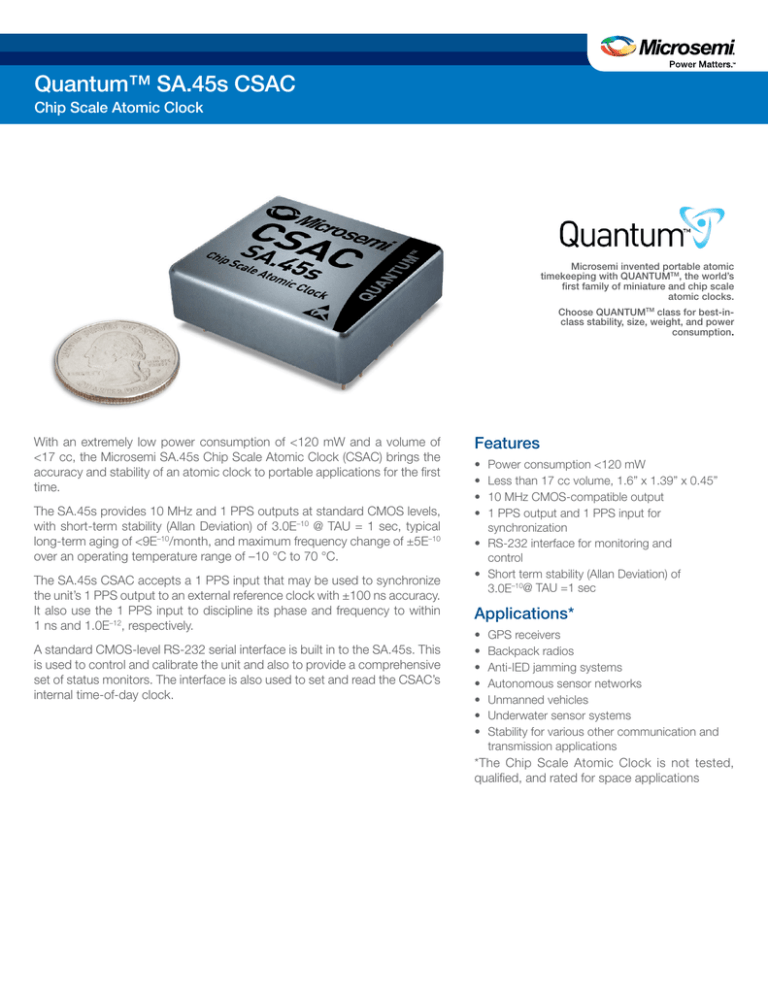
With an extremely low power consumption of <120 mW and a volume of
<17 cc, the Microsemi SA.45s Chip Scale Atomic Clock (CSAC) brings the
accuracy and stability of an atomic clock to portable applications for the first
time.
The SA.45s provides 10 MHz and 1 PPS outputs at standard CMOS levels,
with short-term stability (Allan Deviation) of 3.0E–10 @ TAU = 1 sec, typical
long-term aging of <9E–10/month, and maximum frequency change of ±5E–10
over an operating temperature range of –10 °C to 70 °C.
The SA.45s CSAC accepts a 1 PPS input that may be used to synchronize
the unit’s 1 PPS output to an external reference clock with ±100 ns accuracy.
It also use the 1 PPS input to discipline its phase and frequency to within
1 ns and 1.0E–12, respectively.
A standard CMOS-level RS-232 serial interface is built in to the SA.45s. This
is used to control and calibrate the unit and also to provide a comprehensive
set of status monitors. The interface is also used to set and read the CSAC’s
internal time-of-day clock.
Features
•
•
•
•
Power consumption <120 mW
Less than 17 cc volume, 1.6” x 1.39” x 0.45”
10 MHz CMOS-compatible output
1 PPS output and 1 PPS input for
synchronization
• RS-232 interface for monitoring and
control
• Short term stability (Allan Deviation) of
3.0E–10@ TAU =1 sec
Applications*
•
•
•
•
•
•
•
GPS receivers
Backpack radios
Anti-IED jamming systems
Autonomous sensor networks
Unmanned vehicles
Underwater sensor systems
Stability for various other communication and
transmission applications
*The Chip Scale Atomic Clock is not tested,
qualified, and rated for space applications
Quantum™ SA.45s CSAC
Chip Scale Atomic Clock
Options to Meet a Wider Range of Applications
Following are the different SA.45s CSAC options with there
output frequencies.
Options
001
003
004
006
Output Frequency
For other output frequencies please contact Microsemi
for details.
The Chip Scale Atomic Clock is not tested, qualified, and
rated for space applications.
10 MHz
16.384 MHz
10.24 MHz
5 MHz
Mechanical Interface
Pin Description
Pin Number
1
2
3
4
I.D.
Tune
N/A
N/A
BITE
5
Tx
6
7
8
9
10
11
12
Rx
Vcc
GND
1 PPS IN
1 PPS OUT
N/A
10 MHz OUT
6
7
5
8
4
9
10
12
1
Bottom View
Quantum™ SA.45s CSAC Option 001
Part number 090-02984-001
Specification
All specifications at 25 °C, Vcc = 3.3 VDC unless otherwise
specified.
Electrical Specification
RF Output
•
•
•
•
•
Frequency10 MHz
FormatCMOS
Amplitude
0 V to Vcc
Load impedance
1 MΩ
Quantity 1
1 PPS Output
• Rise/fall time (10%-90%) at load capacitance 10 pF
<10 ns
• Pulse width 100 µs • Level 0 V to Vcc 2.80 V
• Logic High (VoH) min
0.30 V
• Logic Low (VoL) max
• Load impedance
1 MΩ
• Quantity 1
1 PPS Input
•
•
•
•
•
Format
Rising edge Low level <0.5 V High level
2.5 V to Vcc Input impedance 1 MΩ Quantity 1
Serial Communications
•
•
•
•
Protocol Format Tx/Rx impedance Baud rate RS232 CMOS 0 V to Vcc 1 MΩ 57600
•
•
•
•
•
(max. rate of change
0.5 °C/minute)±5x10–10
Frequency change over
allowable input voltage range ±4x10⁻¹⁰ Magnetic sensitivity (≤2.0 Gauss) ±9x10–11/Gauss
Radiated emissions
Compliant to FCC part 15, Class B, when mounted properly onto host PCB.
Vibration Maintains lock under
MIL-STD-810, Method 514.5, Procedure 1, 7.7 grms
Humidity 0 to 95% RH per MIL-STD-810, Method 507.4.
Storage and Transport (non-operating)
• Temperature • Shock (1 ms half-sine) • Vibration Performance Parameters
Stability (Allan Deviation) ADEV
•
•
•
•
TAU = 1 sec TAU = 10 sec
TAU = 100 sec TAU = 1000 sec
•
•
•
•
•
•
1 Hz<–50 dBc/Hz
10 Hz
<–70 dBc/Hz 100 Hz
<–113 dBc/Hz 1000 Hz
<–128 dBc/Hz 10000 Hz
<–135 dBc/Hz 100,000 Hz
<–140 dBc/Hz
Frequency Accuracy
• Format CMOS 0 V to Vcc • Load impedance 1 MΩ • Logic 0 = Normal operation
1 = Alarm
•
•
•
•
•
• Operating <120 mW • Warmup<140 mW
3.3 ± 0.1 VDC
• Input voltage (Vcc) Physical Specifications
• Size • Weight • MTBF 1.6” x 1.39” x 0.45”
<35 g >100,000 hours
Environmental Specification
Operating
• Operating temperature • Maximum frequency change
over operating temp range
–10 °C to 70 °C
3.0x10⁻¹⁰ 1.0x10⁻¹⁰ 3.0x10⁻¹¹ 1.0x10⁻¹¹
RF Output Phase Noise (SSB)
Built-in Test Equipment (BITE) output
Power Input
–55 °C to 85 °C 1000 g MIL-STD-810, Method 514.5, Procedure 1, 7.7 grms
Maximum offset at shipment Maximum retrace (48 hrs off) Aging, monthly* Aging, yearly* 1 PPS Sync.
±5x10–11 ±5x10⁻¹⁰ <9x10⁻¹⁰ typical**
<1x10⁻⁸ typical**
±100 ns (*After 30 days of continuous operation)
Digital Tuning
• Range ±2x10⁻⁸
• Resolution 1x10–12
Analog Tuning
• Range ±2.2x10⁻⁸ • Resolution 1x10–11 • Input
0-2.5 V into 100 kΩ
Warm-up Time<180 s
Solder
Hand solder using 63/37 Tin/Lead Solder with maximum
soldering tip of 329 °C (625 °F)
** All CSAC units are tested for aging specs as per the datasheet and meet the specs at the time of shipment. However, continuous operation of CSAC over extended period of time
may yield unpredictable aging performance, resulting in failure to meet the aging specs and may not be suitable for certain applications.
Quantum™ SA.45s CSAC Option 003
Part number 090-02984-003
Specification
All specifications at 25 °C, Vcc = 3.3 VDC unless otherwise
specified.
Electrical Specification
RF Output
•
•
•
•
•
Frequency16.384 MHz
Format CMOS
Amplitude
0 V to Vcc
Load impedance 1 MΩ
Quantity 1
1 PPS Output
• Rise/fall time (10%-90%) at
load capacitance 10 pF <10 ns
• Pulse width
97.656 μs
• Level 0 V to Vcc
• Logic High (VOH) min 2.80 V
0.30 V
• Logic Low (VOL) max • Load impedance 1 MΩ
• Quantity 1
1 PPS Input
•
•
•
•
•
Format
Rising edge
Low level <0.5 V
High level 2.5 V to Vcc
Input impedance 1 MΩ
Quantity 1
Serial Communications
•
•
•
•
Protocol
Format Tx/Rx impedance Baud rate RS-232
CMOS 0 V to Vcc
1 MΩ
57600
•
•
•
•
•
(max. rate of change
0.5 °C/minute)±5x10–10
Frequency change over
allowable input voltage range ±4x10⁻¹⁰ Magnetic sensitivity (≤2.0 Gauss) ±9x10–11/Gauss
Radiated emissions
Compliant to FCC part 15, Class B, when mounted properly onto host PCB.
Vibration Maintains lock under
MIL-STD-810, Method 514.5, Procedure 1, 7.7 grms
Humidity 0 to 95% RH per MIL-STD-810, Method 507.4.
Storage and Transport (non-operating)
• Temperature • Shock (1 ms half-sine) • Vibration Performance Parameters
Stability (Allan Deviation) ADEV
•
•
•
•
TAU = 1 sec TAU = 10 sec
TAU = 100 sec TAU = 1000 sec
•
•
•
•
•
•
1 Hz<–46 dBc/Hz
10 Hz
<–66 dBc/Hz 100 Hz
<–110 dBc/Hz 1000 Hz
<–128 dBc/Hz 10000 Hz
<–135 dBc/Hz 100,000 Hz
<–140 dBc/Hz
Frequency Accuracy
• Format CMOS 0 V to Vcc
• Load impedance 1 MΩ
• Logic 0 = Normal operation
1 = Alarm
•
•
•
•
•
• Operating • Warmup • Input Voltage (Vcc) ±5x10–11 ±5x10⁻¹⁰ <9x10⁻¹⁰ typical**
<1x10⁻⁸ typical**
±100 ns (*After 30 days of continuous operation)
Digital Tuning
1.6” x 1.39” x 0.45”
<35 g
>100,000 hours
Analog Tuning
Environmental Specification
Operating
• Operating temperature • Maximum frequency change
over operating temp range
Maximum offset at shipment Maximum retrace (48 hrs off):
Aging, monthly* Aging, yearly* 1 PPS Sync.
<120 mW
<140 mW
3.3 ± 0.1 VDC
Physical Specifications
• Size • Weight • MTBF 3.0x10⁻¹⁰ 1.0x10⁻¹⁰ 3.0x10⁻¹¹ 1.0x10⁻¹¹
RF Output Phase Noise (SSB)
Built-in Test Equipment (BITE) output
Power Input
–55 °C to 85 °C 1000 g MIL-STD-810, Method 514.5, Procedure 1, 7.7 grms
–10 °C to 70 °C
• Range ±2x10⁻⁸
• Resolution1x10–12
• Range ±2.2x10⁻⁸ • Resolution 1x10–11 • Input
0-2.5 V into 100 kΩ
Warm-up Time<180 s
Solder
Hand solder using 63/37 Tin/Lead Solder with maximum
soldering tip of 329 °C (625 °F)
** All CSAC units are tested for aging specs as per the datasheet and meet the specs at the time of shipment. However, continuous operation of CSAC over extended period of time
may yield unpredictable aging performance, resulting in failure to meet the aging specs and may not be suitable for certain applications.
Quantum™ SA.45s CSAC Option 004
Part number 090-02984-004
Specification
All specifications at 25 °C, Vcc = 3.3 VDC unless otherwise
specified.
Electrical Specification
RF Output
•
•
•
•
•
Frequency10.24 MHz
Format CMOS
Amplitude
0 V to Vcc
Load impedance 1 MΩ
Quantity 1
1 PPS Output
• Rise/fall time (10%-90%) at
load capacitance 10 pF <10 ns
• Pulse width
100 μs
• Level 0 V to Vcc
• Logic High (VOH) min 2.80 V
0.30 V
• Logic Low (VOL) max • Load impedance 1 MΩ
• Quantity 1
1 PPS Input
•
•
•
•
•
Format
Rising edge
Low level <0.5 V
High level
2.5 V to Vcc
Input impedance 1 MΩ
Quantity 1
Serial Communications
•
•
•
•
Protocol
Format Tx/Rx impedance Baud rate RS-232
CMOS 0 V to Vcc
1 MΩ
57600
•
•
•
•
•
(max. rate of change
0.5 °C/minute)±5x10–10
Frequency change over
allowable input voltage range ±4x10⁻¹⁰ Magnetic sensitivity (≤2.0 Gauss) ±9x10–11/Gauss
Radiated emissions
Compliant to FCC part 15, Class B, when mounted properly onto host PCB.
Vibration Maintains lock under
MIL-STD-810, Method 514.5, Procedure 1, 7.7 grms
Humidity 0 to 95% RH per MIL-STD-810, Method 507.4.
Storage and Transport (non-operating)
• Temperature • Shock (1 ms half-sine) • Vibration Performance Parameters
Stability (Allan Deviation) ADEV
•
•
•
•
TAU = 1 sec TAU = 10 sec
TAU = 100 sec TAU = 1000 sec
•
•
•
•
•
•
1 Hz<–50 dBc/Hz
10 Hz
<–70 dBc/Hz 100 Hz
<–113 dBc/Hz 1000 Hz
<–128 dBc/Hz 10000 Hz
<–135 dBc/Hz 100,000 Hz
<–140 dBc/Hz
Frequency Accuracy
• Format CMOS 0 V to Vcc
• Load impedance 1 MΩ
• Logic 0 = Normal operation
1 = Alarm
•
•
•
•
•
• Operating • Warmup • Input Voltage (Vcc) ±5x10–11 ±5x10⁻¹⁰ <9x10⁻¹⁰ typical**
<1x10⁻⁸ typical**
±100 ns (*After 30 days of continuous operation)
Digital Tuning
1.6” x 1.39” x 0.45”
<35 g
>100,000 hours
Analog Tuning
Environmental Specification
Operating
• Operating temperature • Maximum frequency change
over operating temp range
Maximum offset at shipment Maximum retrace (48 hrs off) Aging, monthly* Aging, yearly* 1 PPS Sync.
<120 mW
<140 mW
3.3 ± 0.1 VDC
Physical Specifications
• Size • Weight • MTBF 3.0x10⁻¹⁰ 1.0x10⁻¹⁰ 3.0x10⁻¹¹ 1.0x10⁻¹¹
RF Output Phase Noise (SSB)
Built-in Test Equipment (BITE) output
Power Input
–55 °C to 85 °C 1000 g MIL-STD-810,Method 514.5, Procedure 1, 7.7 grms
–10 °C to 70 °C
• Range ±2x10⁻⁸
• Resolution 1x10–12
• Range ±2.2x10⁻⁸ • Resolution 1x10–11 • Input
0-2.5 V into 100 kΩ
Warm-up Time<180 s
Solder
Hand solder using 63/37 Tin/Lead Solder with maximum
soldering tip of 329 °C (625 °F)
** All CSAC units are tested for aging specs as per the datasheet and meet the specs at the time of shipment. However, continuous operation of CSAC over extended period of time
may yield unpredictable aging performance, resulting in failure to meet the aging specs and may not be suitable for certain applications.
Quantum™ SA.45s CSAC Option 006
Part number 090-02984-006
Specification
All specifications at 25 °C, Vcc = 3.3 VDC unless otherwise
specified.
Electrical Specification
RF Output
•
•
•
•
•
Frequency5 MHz
Format CMOS
Amplitude
0 V to Vcc
Load impedance 1 MΩ
Quantity 1
1 PPS Output
• Rise/fall time (10%-90%) at
load capacitance 10 pF <10 ns
• Pulse width
100 μs
• Level 0 V to Vcc
• Logic High (VOH) min 2.80 V
0.30 V
• Logic Low (VOL) max • Load impedance 1 MΩ
• Quantity 1
1 PPS Input
•
•
•
•
•
Format
Rising edge
Low level <0.5 V
High level 2.5 V to Vcc
Input impedance 1 MΩ
Quantity 1
Serial Communications
•
•
•
•
Protocol
Format Tx/Rx impedance Baud rate RS-232
CMOS 0 V to Vcc
1 MΩ
57600
Environmental Specification
Operating
• Operating temperature –10 °C to 70 °C
• Maximum frequency change
over operating temp range
(max. rate of change
0.5 °C/minute)±5x10–10 • Frequency change over
allowable input voltage range ±4x10⁻¹⁰ • Magnetic sensitivity (≤2.0 Gauss) ±9x10–11/Gauss
• Radiated emissions
Compliant to FCC part 15, Class B, when mounted properly onto host PCB.
• Vibration Maintains lock under
MIL-STD-810, Method 514.5, Procedure 1, 7.7 grms
• Humidity 0 to 95% RH per MIL-STD-810, Method 507.4.
Storage and Transport (non-operating)
• Temperature • Shock (1 ms half-sine) • Vibration Performance Parameters
Stability (Allan Deviation) ADEV
•
•
•
•
TAU = 1 sec TAU = 10 sec
TAU = 100 sec TAU = 1000 sec
• Format CMOS 0 V to Vcc
• Load impedance 1 MΩ
• Logic 0 = Normal operation
1 = Alarm
Power Input
Frequency Accuracy
• Operating • Warmup • Input Voltage (Vcc) <120 mW
<140 mW
3.3 ± 0.1 VDC
Physical Specifications
• Size • Weight • MTBF 1.6” x 1.39” x 0.45”
<35 g
>100,000 hours
3.0x10⁻¹⁰ 1.0x10⁻¹⁰ 3.0x10⁻¹¹ 1.0x10⁻¹¹
RF Output Phase Noise (SSB)
•
•
•
•
•
•
Built-in Test Equipment (BITE) output
–55 °C to 85 °C 1000 g MIL-STD-810,Method 514.5, Procedure 1, 7.7 grms
•
•
•
•
•
1 Hz<–53 dBc/Hz
10 Hz
<–73 dBc/Hz 100 Hz
<–116 dBc/Hz 1000 Hz
<–131 dBc/Hz 10000 Hz
<–138 dBc/Hz 100,000 Hz
<–140 dBc/Hz
Maximum offset at shipment Maximum retrace (48 hrs off) Aging, monthly* Aging, yearly* 1 PPS Sync.
±5x10–11 ±5x10⁻¹⁰ <9x10⁻¹⁰ typical**
<1x10⁻⁸ typical**
±100 ns (*After 30 days of continuous operation)
** All CSAC units are tested for aging specs as per the datasheet and meet the specs at the time of shipment. However, continuous operation of CSAC over extended period of time
may yield unpredictable aging performance, resulting in failure to meet the aging specs and may not be suitable for certain applications.
Quantum™ SA.45s CSAC Option 006 cont.
Part number 090-02984-006
Digital Tuning
• Range ±2x10⁻⁸
• Resolution 1x10–12
Analog Tuning
• Range ±2.2x10⁻⁸ • Resolution 1x10–11 • Input
0-2.5 V into 100 kΩ
Warm-up Time<180 s
Solder
Hand solder using 63/37 Tin/Lead Solder with maximum soldering tip of 329 °C (625 °F)
Microsemi Corporate Headquarters
One Enterprise, Aliso Viejo, CA 92656 USA
Within the USA: +1 (800) 713-4113
Outside the USA: +1 (949) 380-6100
Fax: +1 (949) 215-4996
Email: sales.support@microsemi.com
www.microsemi.com
©2016 Microsemi Corporation. All rights reserved.
Microsemi and the Microsemi logo are registered
trademarks of Microsemi Corporation. All other
trademarks and service marks are the property
of their respective owners.
Microsemi Corporation (Nasdaq: MSCC) offers a comprehensive portfolio of semiconductor and system solutions for aerospace
& defense, communications, data center and industrial markets. Products include high-performance and radiation-hardened
analog mixed-signal integrated circuits, FPGAs, SoCs and ASICs; power management products; timing and synchronization
devices and precise time solutions, setting the world’s standard for time; voice processing devices; RF solutions; discrete
components; enterprise storage and communication solutions, security technologies and scalable anti-tamper products;
Ethernet solutions; Power-over-Ethernet ICs and midspans; as well as custom design capabilities and services. Microsemi is
headquartered in Aliso Viejo, California and has approximately 4,800 employees globally. Learn more at www.microsemi.com.
Microsemi makes no warranty, representation, or guarantee regarding the information contained herein or the suitability of its products and services for any
particular purpose, nor does Microsemi assume any liability whatsoever arising out of the application or use of any product or circuit. The products sold
hereunder and any other products sold by Microsemi have been subject to limited testing and should not be used in conjunction with mission-critical equipment
or applications. Any performance specifications are believed to be reliable but are not verified, and Buyer must conduct and complete all performance and other
testing of the products, alone and together with, or installed in, any end-products. Buyer shall not rely on any data and performance specifications or parameters
provided by Microsemi. It is the Buyer’s responsibility to independently determine suitability of any products and to test and verify the same. The information
provided by Microsemi hereunder is provided “as is, where is” and with all faults, and the entire risk associated with such information is entirely with the Buyer.
Microsemi does not grant, explicitly or implicitly, to any party any patent rights, licenses, or any other IP rights, whether with regard to such information itself
or anything described by such information. Information provided in this document is proprietary to Microsemi, and Microsemi reserves the right to make any
changes to the information in this document or to any products and services at any time without notice.
DS/SA.45s/CSAC/0916 900-00744-000 A


