Analog Devices: 5B Series Overview : 5B Series : IOS Subsystems : Market Solutions
Search:
Parametric Search
|
Replacement Parts Search
Page 1 of 5
View Cart
|
My Account
|
Log
Home > Other > IOS Subsystems
Contact Us
Product Categories
Amplifiers and
Comparators
|
P
AC1367 Voltage Input
5B Series Overview | Available 5B Series Modules | 5B Series Backplanes | 5B and 6B Series Power Supplies
5B Series Accessories | 5B Series Configuration Guide | Outline Drawings | All Series Modules
Analog to Digital
Converters
Select a topic
Digital to Analog
Converters
Analog Microcontrollers
Functional Description
Embedded Processing &
DSP
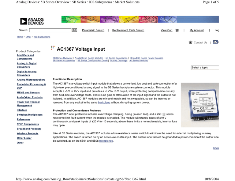
The AC1367 is a voltage-switch input module that allows a convenient, low cost and safe connection of a
high-level pre-conditioned analog signal to the 5B Series backplane system connector. This module
accepts a -5 V to +5 V input and provides a -5 V to +5 V output, while protecting computer-side circuitry
from field-side overvoltage faults. There is no gain or attenuation of the input signal and the output is not
isolated. In addition, AC1367 modules are mix-and-match and hot swappable, so can be inserted or
removed from any socket in the same backplane without disrupting system power.
MEMS and Sensors
Audio/Video Products
Power and Thermal
Management
Interface
Switches/Multiplexers
References
RF/IF Components
Protection and Convenience Features
The AC1367 input protection includes overvoltage clamping, fusing (in each line), and a 250
series
resistor to limit fault current when the module is enabled. The module withstands inputs of ±10 V
continuously, and peak inputs of ±20 V for 10 seconds; above these limits a nonreplaceable, internal fuse
may open.
Broadband Products
Wireless Products
Other Linear
Other
Like all 5B Series modules, the AC1367 includes a low-resistance series switch to eliminate the need for external multiplexing in many
applications. The switch is turned on by an active-low enable input. The enable input should be grounded to power common if the output need
be switched, as on the 5B01 and 5B08 backplanes.
back
http://www.analog.com/Analog_Root/static/marketSolutions/ios/catalog/5b/5bac1367.html
10/8/2004
Analog Devices: 5B Series Overview : 5B Series : IOS Subsystems : Market Solutions
Page 2 of 5
Figure 1. AC1367 Functional Block Diagram
Input Types
-5 V to +5 V
Output Ranges
-5 V to +5 V
Figure 2. AC1367 Input Field Connections
back
AC1367 Models Available
Model Input Range Output Range
Order Now AC1367 -5 V to +5 V
-5 V to +5 V)
http://www.analog.com/Analog_Root/static/marketSolutions/ios/catalog/5b/5bac1367.html
10/8/2004
Analog Devices: 5B Series Overview : 5B Series : IOS Subsystems : Market Solutions
Page 3 of 5
back
AC1367 Specifications
(typical @ +25°C and Vs = +5V dc
Description
Model AC1367
Input Ranges
Standard Range
-5 V to +5 V
Custom Ranges
Not Available
-5 V to +5 V
Output Range
Maximum Voltage at Input
Low1
0.0 V
Maximum Current into Input Low2
±20 mA
Maximum Current into Input High2
±20 mA
Maximum Output When Input Is Overrange
±10 V
Feedthrough, Input-to-Output @ 1 kHz, Rload = 50 k
-100 dB
Input-to-Output Resistance, when enabled
250
Input Resistance
Power On
10 M
Power Off
200
Overrange
200
Noise
http://www.analog.com/Analog_Root/static/marketSolutions/ios/catalog/5b/5bac1367.html
10/8/2004
Analog Devices: 5B Series Overview : 5B Series : IOS Subsystems : Market Solutions
Page 4 of 5
Output, 100 kHz Bandwidth
300 µV peak-peak
Bandwidth, -3 dB
500 kHz
Output Rise Time, 10% to 90% Span
500 ns
Input Protection
±10 V Continuous
±20 V for 10 seconds
Output Resistance
250
Voltage Output Protection
Continuous Short to Ground
Output Selection Time
6 µs @ Cload = 0 to 2,000 pF
+ Input Source Resistance
Output Enable Control
Max Logic "0"
+1 V
Min Logic "1"
+2.5 V
Max Logic "1"
+36 V
Input Current "0"
0.4 mA
Power Supply
Voltage
+5 V ±5%
Current
6.5 mA
Mechanical Dimensions
2.275" x 2.375" x 0.595"
(57.8 mm x 59.1 mm x 15.1 mm)
Environmental
Temperature Range
Rated Performance
-25°C to +85°C
Operating
-40°C to +85°C
Storage
-40°C to +85°C
Relative Humidity
0 to 95% @ +60°C noncondensing
RFI Susceptibility
±0.5% Span error @ 400 MHz, 5 Watt, 3 ft
1Input
Low is internally connected to the I/O common (refer to block diagram).
High and Input Low are internally fused; the fuse is nonreplaceable.
Specifications subject to change without notice.
2Input
back
Privacy/Security
myAnalog
Contact ADI
Site Map
Registration
Technical Support
Terms of Use
© 1995-2004 Analog Devices, Inc. All Rights Reserved
http://www.analog.com/Analog_Root/static/marketSolutions/ios/catalog/5b/5bac1367.html
10/8/2004
Analog Devices: 5B Series Overview : 5B Series : IOS Subsystems : Market Solutions
Page 5 of 5
This site is optimized for IE 6.0+, NN 7.1, and Mozilla.
http://www.analog.com/Analog_Root/static/marketSolutions/ios/catalog/5b/5bac1367.html
10/8/2004

