Technical Brief
Computing Self and Mutual
Capacitance and Inductance Using
Even and Odd TDR Measurements
Abstract
Lself =
TDR measurement techniques for IC package characterization have been reported extensively and
standardized by JEDEC [1]. In addition, several
techniques utilizing differential TDR measurements
have been reported in [2]. In this paper, we will
present a novel technique for computing self and
mutual inductance and capacitance. This technique
is based on applying computational procedures as
described in [1] to even and odd mode TDR
measurements of the device under test, such as a
connector or IC package.
Introduction
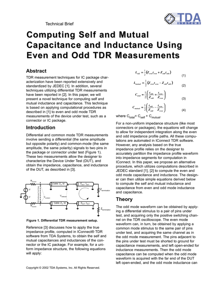
Differential and common mode TDR measurements
involve sending a differential (the same amplitude
but opposite polarity) and common-mode (the same
amplitude, the same polarity) signals to two pins in
the package or connector under test (Figure 1).
These two measurements allow the designer to
characterize the Device Under Test (DUT), and
obtain the impedance, capacitance, and inductance
of the DUT, as described in [3].
Rsource
TDR Oscilloscope Front Panel
Cable: Z 0, td
V
V
Rsource
ZDUT , tDUT
Ztermination
Vincident
Vreflected
Cable: Z 0, td
C total =
C mutual =
2
(Z even teven + Z odd todd )
(1)
1
(Z even t even − Z odd t odd )
2
(2)
t
1 t odd
+ even
2 Z odd Z even
(3)
t
1 t odd
− even
2 Z odd Z even
(4)
where Ctotal= Cself + Cmutual.
For a non-uniform impedance structure (like most
connectors or packages), the equations will change
to allow for independent integration along the even
and odd impedance profile paths. All these computations are automated in IConnect TDR software.
However, any analysis based on the true
impedance profile relies on the designer to
accurately partition the impedance profile waveform
into impedance segments for computation in
IConnect. In this paper, we propose an alternative
procedure, which utilizes computations described in
JEDEC standard [1], [2] to compute the even and
odd mode capacitance and inductance. The designer can then utilize simple equations derived below
to compute the self and mutual inductance and
capacitance from even and odd mode inductance
and capacitance.
Theory
ZDUT , tDUT
Ztermination
Figure 1. Differential TDR measurement setup.
Reference [3] discusses how to apply the true
impedance profile, computed in IConnect® TDR
software from TDA Systems, to obtain the self and
mutual capacitances and inductances of the connector or the IC package. For example, for a uniform impedance structure, the following equations
will apply:
Copyright © 2002 TDA Systems, Inc. All Rights Reserved.
Lmutual =
1
The odd mode waveform can be obtained by applying a differential stimulus to a pair of pins under
test, and acquiring only the positive switching channel on the TDR oscilloscope. The even mode
waveform can, in turn, be obtained by applying a
common mode stimulus to the same pair of pins
under test, and acquiring the same channel as in
the odd mode measurement. The pins adjacent to
the pins under test must be shorted to ground for
capacitance measurements, and left open-ended for
inductance measurements. Then the odd mode
capacitance can be computed when the odd mode
waveform is acquired with the far end of the DUT
left open-ended, and the odd mode inductance can
be computed when the odd mode waveform is
acquired with the far end of the DUT connected to
ground, or at least with the two pins under test connected together, by applying the computational procedure described in JEDEC standard [1], [2]. The
even mode capacitance and inductance can be
computed from the even mode waveform under the
same fixturing conditions using the same computational procedure. Thus, we obtain:
∞
1
Codd =
⋅ ∫ (Wopen − Wodd _ open )dt
2 ⋅ Z0 ⋅V 0
(5)
The following figure shows the measurement setup
for the odd or even mode capacitance
measurement.
1
⋅ (Wopen − Weven _ open )dt
2 ⋅ Z 0 ⋅ V ∫0
Z0
+
v2
_
C2
(6)
In the even mode, there is no the voltage difference
across Cmutual. Therefore, no current flows through
it, making it equivalent to an open circuit. Therefore,
applying equation (6) will give us the self capacitance of the circuit:
Cself = Ceven
(9)
In the odd mode, a virtual ground plane divides the
mutual capacitance into two series capacitances of
2Cm, and the node between them is grounded.
Wopen
C
W TDR
2V
Figure 2. Self-capacitance measurement.
v1
+
C1
I1
At the same time,
∞
Lodd =
Z0
⋅ (Wodd _ short − Wshort ) dt
2 ⋅ V ∫0
Leven =
Z0
⋅ (Weven _ short − Wshort ) dt
2 ⋅ V ∫0
W TDR
L
2 Cmutual
I2
2 Cmutual
(7)
Z0
∞
(8)
2V
Figure 3. Self-inductance measurement.
+
v2
_
C2
Therefore, if we compute the result of equation (5),
we obtain Cself+2Cmutual. Then, Cmutual can be
found as:
Cmutual =
2
Cmutual
2V
where V is the TDR voltage incident at the lead
under test, normally half the TDR source amplitude,
and Z0 equals the characteristic impedance of the
measurement system, 50 Ω for currently available
TDR instruments. For practical purposes, it is not
necessary to integrate to infinity, but only until the
difference between the Wopen and Weven/odd is negligibly small.
W short
C1
I1
I2
∞
Ceven =
v1
+
2V
(Codd − Ceven )
2
(10)
The following figure shows the measurement setup
for the odd or even mode inductance measurement:
- V1 +
Z0
Z0
Lmutual
2V
I1
L1
L2 I2
- V2 +
Z0
It is important to keep in mind that the lumped
models extracted using the equations (9), (10), (18)
and (19) above will only be valid if the electrical
length of the package or connector under test, or
the given segment of this package or connector, is
much shorter than the rise time of the signals propagating through this package or connector:
t
t package < rise
2V
6
(20)
Measurement Examples
We can see that:
di1
V1 = L1
dt
V 2 = L mutual
di 2
+ L mutual
dt
di1
di 2
+ L2
dt
dt
(11)
Since in odd mode with differential stimulus,
V1 = −V 2 , i1 = −i 2 ,and L1 = L 2 = L self we obtain:
V = ( L self − Lmutual )
di
dt
As a measurement example, we measured the
input capacitance of a differential pin pair in a package. The test setup included a test fixture board,
with the socket mounted in the center of the board.
The TDR measurements of the fixture board are
shown in the figure below.
(12)
This equation, following the derivation for the self
inductance of the package lead, gives us:
( Lself − Lmutual ) =
∞
Z0
⋅ (Wodd _ short − Wshort )dt
2 ⋅ V ∫0
(13)
or,
Lself − Lmutual = Lodd
(14)
In even mode, on the other hand, V1 = V2 , i1 = i2 , and
L1 = L 2 = L self , and we obtain:
V = ( Lself + Lmutual )
Figure 4. TDR waveform of the test fixture.
di
dt
(15)
This equation, following the derivation for the self
inductance of the package lead, gives us:
( Lself + Lmutual ) =
∞
Z0
⋅ (Weven _ short − Wshort )dt
2 ⋅ V ∫0
(16)
or,
Lself + Lmutual = Leven
(17)
We can now use the procedure outlined above to
compute the odd mode capacitance using the
differential stimulus and the JEDEC procedure. The
reference waveform is the odd mode waveform on
Channel 1 of the oscilloscope with the socket
empty, and the package waveform is the odd mode
waveform on Channel 1 with the packaged part
inside the socket. The resulting odd mode capacitance, computed using the Cself computation in
IConnect, is 760fF.
Combining equations (14) and (17), we obtain:
Lself =
(Leven + Lodd )
Lmutual =
2
(18)
(Leven − Lodd )
2
(19)
3
Summary and Conclusions
In this paper, we proposed a novel procedure for
computing the parasitics of a connector or a package using the even and odd mode capacitance and
inductance measurements. The advantage of this
new procedure is that it is simple and relatively
error-proof. However, this new procedure allows the
designer to extract only the lumped model for the
interconnect in question. Such lumped model is only
valid when the length of the package or connector
interconnect is much shorter than the rise time of
the signals propagating through this interconnect.
Bibliography
Figure 5. Odd mode capacitance measurement.
We can now compute the even mode capacitance
using the common mode stimulus and the JEDEC
procedure. The reference waveform is the even
mode waveform on Channel 1 of the oscilloscope
with the socket empty, and the package waveform
is the even mode waveform on Channel 1 with the
packaged part inside the socket. The resulting even
mode capacitance, computed using the Cself
computation in IConnect, is 360fF.
Then, we can apply equations (9) and (10), which
give Cself of 360fF and Cmutual of 200fF.
[1] Guideline for Measurement of Electronic
Package Inductance and Capacitance Model
Parameters, − JEDEC Publication #123, JC-15
Committee, October 1995
[2] D.A. Smolyansky, "TDR Techniques for
Characterization and Modeling of Electronic
Packaging," − High Density Interconnect Magazine,
March and April 2001, 2 parts (TDA Systems
Application Note PKGM-0101)
[3] D. A. Smolyansky, S. D. Corey, "Characterization
of Differential Interconnects from Time Domain
Reflectometry Measurements," − Microwave
Journal, Vol. 43, No. 3, pp. 68-80 (TDA Systems
application note DIFF-1099)
Figure 6. Even mode capacitance measurement.
© 2002 TDA Systems, Inc. All Rights Reserved
4000 Kruse Way Place, 2-300 Lake Oswego, OR 97035, USA
Telephone: (503) 246-2272 Fax: (503) 246-2282
E-mail: info@tdasystems.com Web site: www.tdasystems.com
The Interconnect Analysis Company™
4
CECO-0703
Data subject to
change without notice


![ )] (](http://s2.studylib.net/store/data/010418727_1-2ddbdc186ff9d2c5fc7c7eee22be7791-300x300.png)

