LD39030
300 mA very low quiescent current linear regulator IC
Datasheet - production data
Applications
Mobile phones
Tablets
Digital still cameras (DSC)
Cordless phones and similar batterypowered systems
Portable media players
Description
Features
Input voltage from 1.5 to 5.5 V
Ultra low dropout voltage (300 mV typ. at
300 mA load)
Very low quiescent current (20 µA typ. at no
load, 0.03 µA typ. in off mode)
Output voltage tolerance: ± 0.5 % (A
version) or ± 2.0 % @ 25 °C (standard
version)
300 mA guaranteed output current
High PSRR (80 dB@1 kHz, 50 db@100
kHz)
Wide range of output voltages available on
request: from 0.8 V up to 5.0 V in 50 mV
step
Logic-controlled electronic shutdown
Internal soft-start
Optional output voltage discharge feature
Compatible with ceramic capacitor
COUT = 0.47 µF
Internal constant current and thermal
protections
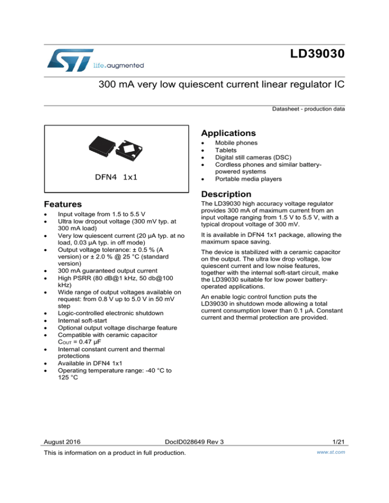
Available in DFN4 1x1
Operating temperature range: -40 °C to
125 °C
August 2016
The LD39030 high accuracy voltage regulator
provides 300 mA of maximum current from an
input voltage ranging from 1.5 V to 5.5 V, with a
typical dropout voltage of 300 mV.
It is available in DFN4 1x1 package, allowing the
maximum space saving.
The device is stabilized with a ceramic capacitor
on the output. The ultra low drop voltage, low
quiescent current and low noise features,
together with the internal soft-start circuit, make
the LD39030 suitable for low power batteryoperated applications.
An enable logic control function puts the
LD39030 in shutdown mode allowing a total
current consumption lower than 0.1 µA. Constant
current and thermal protection are provided.
DocID028649 Rev 3
This is information on a product in full production.
1/21
www.st.com
Contents
LD39030
Contents
1
Diagram ............................................................................................ 3
2
Pin configuration ............................................................................. 4
3
Typical application .......................................................................... 5
4
5
Maximum ratings ............................................................................. 6
Electrical characteristics ................................................................ 7
6
Application information .................................................................. 9
6.1
Soft start function .............................................................................. 9
6.2
Output discharge function ................................................................. 9
6.3
Input and output capacitors ............................................................... 9
7
Typical characteristics .................................................................. 10
8
Package information ..................................................................... 15
8.1
DFN4 1x1 package information ....................................................... 16
9
Ordering information..................................................................... 19
10
Revision history ............................................................................ 20
2/21
DocID028649 Rev 3
LD39030
1
Diagram
Diagram
Figure 1: Block diagram
The output discharge MOSFET is optional.
DocID028649 Rev 3
3/21
Pin configuration
2
LD39030
Pin configuration
Figure 2: Pin connection (top view)
Table 1: Pin description
4/21
Pin n° DFN4 1x1
Symbol
Function
1
OUT
Output voltage
2
GND
Common ground
3
EN
Enable pin logic input: Low = shutdown, High = active
4
IN
Input voltage
Thermal pad
GND
Connect to GND on the PCB
DocID028649 Rev 3
LD39030
3
Typical application
Typical application
Figure 3: Typical application circuits
DocID028649 Rev 3
5/21
Maximum ratings
4
LD39030
Maximum ratings
Table 2: Absolute maximum ratings
Symbol
Parameter
VIN
Input voltage
Value
Unit
- 0.3 to 7
V
- 0.3 to VIN + 0.3
V
- 0.3 to 7
V
VOUT
Output voltage
VEN
Enable input voltage
IOUT
Output current
Internally limited
mA
Power dissipation
Internally limited
mW
PD
TSTG
Storage temperature range
- 40 to 150
°C
TOP
Operating junction temperature range
- 40 to 125
°C
Absolute maximum ratings are those values beyond which damage to the device
may occur. Functional operation under these conditions is not implied. All values
are referred to GND.
Table 3: Thermal data
Symbol
RthJA
Parameter
Thermal resistance junction-ambient
Value
Unit
250
°C/W
Table 4: ESD Performance
Symbol
ESD
6/21
Parameter
ESD Protection voltage
DocID028649 Rev 3
Test conditions
Value
Unit
HBM
4
kV
MM
400
V
CDM
500
V
LD39030
5
Electrical characteristics
Electrical characteristics
TJ = 25 °C, VIN = VOUT(NOM) + 1 V , CIN = COUT = 1 µF, IOUT = 1 mA, VEN = VIN, unless
otherwise specified.
Table 5: Electrical characteristics
Symbol
Parameter
Test conditions
Min.
Typ.
Max.
Unit
1.5
5.5
V
VIN
Operating input
voltage
VOUT accuracy
(LD39030T,
LD39030DT)
IOUT = 1 mA, TJ = 25 °C
-2
2
%
VOUT
IOUT = 1 mA,
-40 °C < TJ < 125 °C
-3
3
%
VOUT accuracy
(LD39030AT,
LD39030ADT)
IOUT = 1 mA, TJ = 25 °C
-0.5
0.5
%
IOUT = 1 mA,
-40 °C < TJ < 125 °C
-1.5
1.5
%
VOUT
∆VOUT
∆VOUT
VDROP
eN
SVR
Static line
regulation(1)
Static load regulation
Dropout voltage
Output noise voltage
Supply voltage
rejection
VOUT(NOM) + 1 V ≤ VIN ≤ 5.5 V,
IOUT = 10 mA
0.02
-40 °C < TJ < 125 °C
%/V
0.2
IOUT = 0 mA to 300 mA
18
-40 °C < TJ < 125 °C
mV
0.01
IOUT = 30 mA,VOUT = 2.8 V
35
IOUT = 300 mA, VOUT = 2.8 V
-40 °C < TJ < 125 °C
330
10 Hz to 100 kHz,
IOUT = 10 mA
45
VIN = VOUT(NOM)+ 1 V +/- VRIPPLE
VRIPPLE = 0.2 V Freq .=1 kHz
IOUT = 30 mA
80
%/mA
mV
µVRMS/V
dB
VIN = VOUT(NOM)+ 1 V +/- VRIPPLE
VRIPPLE = 0.2 V
Freq. = 100 kHz
IOUT = 30 mA
55
IOUT = 0 mA
20
IOUT = 300 mA
130
Standby Current
VIN input current in OFF
MODE: VEN = GND
0.03
ISC
Short circuit current
RL = 0
480
mA
RON
Output voltage
discharge MOSFET
(only on LD39030DT,
LD39030ADT)
100
Ω
Enable input logic
low
VIN = 1.5 V to 5.5 V
-40 °C < TJ < 125 °C
Enable input logic
high
VIN = 1.5 V to 5.5 V
-40 °C < TJ < 125 °C
Enable pin input
current
VEN = VIN
IQ
IStandby
VEN
IEN
Quiescent current
DocID028649 Rev 3
40
1
µA
µA
0.4
V
1
100
nA
7/21
Electrical characteristics
Symbol
TON(2)
TSHDN
COUT
LD39030
Parameter
Test conditions
Min.
Typ.
Turn on time
100
Thermal shutdown
160
Hysteresis
20
Capacitance (see Figure 17:
"Stability area vs. (COUT,
ESR)")
Output capacitor
0.47
Max.
Unit
µs
°C
22
µF
Notes:
(1)Not
applicable for VOUT(NOM) > 4.5 V
(2)Turn-on
time is time measured between the enable input just exceeding VEN high value and the output voltage
just reaching 95 % of its nominal value
8/21
DocID028649 Rev 3
LD39030
Application information
6
Application information
6.1
Soft start function
The LD39030 has an internal soft start circuit. By increasing the startup time up to 100µs,
without the need of any external soft start capacitor, this feature is able to keep the
regulator inrush current at startup under control.
6.2
Output discharge function
The LD39030 integrates a MOSFET connected between Vout and GND. This transistor is
activated when the EN pin goes to low logic level and has the function to quickly discharge
the output capacitor when the device is disabled by the user.
The device is available with or without auto-discharge feature.
See Section 9: "Ordering information" for more details.
6.3
Input and output capacitors
The LD39030 requires external capacitors to assure the regulator control loop stability.
Any good quality ceramic capacitor can be used but, the X5R and the X7R are suggested
since they guarantee a very stable combination of capacitance and ESR overtemperature.
Locating the input/output capacitors as closer as possible to the relative pins is
recommended.
The LD39030 requires an input capacitor with a minimum value of 1 μF.
This capacitor must be located as closer as possible to the input pin of the device and
returned to a clean analog ground.
The control loop of the LD39030 is designed to work with an output ceramic capacitor.
This capacitor must meet the requirements of minimum capacitance and equivalent series
resistance (ESR), as shown in Figure 17: "Stability area vs. (COUT, ESR)". To assure
stability, the output capacitor must maintain its ESR and capacitance in the stable region,
over the full operating temperature range.
The LD39030 shows stability with a minimum effective output capacitance of 220 nF.
However, to keep stability in all operating conditions (temperature, input voltage and load
variations), a minimum output capacitor of 0.47 µF is recommended.
The suggested combination of 1 μF input and output capacitors offers a good compromise
among the stability of the regulator, optimum transient response and total PCB area
occupation.
DocID028649 Rev 3
9/21
Typical characteristics
7
LD39030
Typical characteristics
(CIN = COUT = 1 µF, VEN to VIN, TJ = 25°C unless otherwise specified)
10/21
Figure 4: Output voltage vs. temperature
(IOUT = 1 mA)
Figure 5: Output voltage vs. temperature
(IOUT = 200 mA)
Figure 6: Line regulation vs. temperature
Figure 7: Load regulation vs. temperature
DocID028649 Rev 3
LD39030
Typical characteristics
Figure 8: Quiescent current vs. temperature
(IOUT = 0 mA)
Figure 9: Quiescent current vs. temperature
(IOUT = 200 mA)
Figure 10: Shutdown current vs. temperature
Figure 11: Quiescent current vs. load current
Figure 12: Quiescent current vs. input voltage
Figure 13: Dropout voltage vs. temperature
DocID028649 Rev 3
11/21
Typical characteristics
LD39030
Figure 14: Supply voltage rejection vs. frequency
Figure 15: Supply voltage rejection vs. input voltage
Figure 16: Output noise spectral density
Figure 17: Stability area vs. (COUT, ESR)
Figure 18: Enable startup (VOUT = 1 V)
Figure 19: Enable startup (VOUT = 5 V)
12/21
DocID028649 Rev 3
LD39030
Typical characteristics
Figure 20: Turn-on time (VOUT = 1 V)
Figure 21: Turn-off time (VOUT = 1 V)
Figure 22: Turn-on time (VOUT = 5 V)
Figure 23: Turn-off time (VOUT = 5 V)
Figure 24: Line transient (VOUT = 1 V)
Figure 25: Line transient (VOUT = 5 V)
DocID028649 Rev 3
13/21
Typical characteristics
LD39030
Figure 26: Load transient (VOUT = 1 V)
14/21
Figure 27: Load transient (VOUT = 5 V)
DocID028649 Rev 3
LD39030
8
Package information
Package information
In order to meet environmental requirements, ST offers these devices in different grades of
ECOPACK® packages, depending on their level of environmental compliance. ECOPACK ®
specifications, grade definitions and product status are available at: www.st.com.
ECOPACK® is an ST trademark.
DocID028649 Rev 3
15/21
Package information
8.1
LD39030
DFN4 1x1 package information
Figure 28: DFN4 1x1 package outline
16/21
DocID028649 Rev 3
LD39030
Package information
Table 6: DFN4 1x1 mechanical data
mm.
Dim.
Min.
Typ.
Max.
A
0.34
0.37
0.40
A1
0
0.02
0.05
A3
0.10
b
0.17
0.22
0.27
D
0.95
1.00
1.05
D2
0.43
0.48
0.53
E
0.95
1.00
1.05
E2
0.43
0.48
0.53
e
0.65
L
0.20
K
0.15
DocID028649 Rev 3
0.25
0.30
17/21
Package information
LD39030
Figure 29: DFN4 1x1 recommended footprint
18/21
DocID028649 Rev 3
LD39030
9
Ordering information
Ordering information
Table 7: Order code
Order code
Output voltage (V)
Auto-discharge
1.8
Yes
LD39030DTPU18R
LD39030ADTPU18R
LD39030DTPU25R
2.5
LD39030DTPU28R
LD39030DTPU30R
3.3
DocID028649 Rev 3
X7
0.5
W7
2
XA
0.5
WA
2
XC
0.5
WC
2
XF
0.5
WF
2
XJ
Yes
LD39030ADTPU30R
LD39030DTPU33R
2
Yes
LD39030ADTPU28R
3.0
Marking
Yes
LD39030ADTPU25R
2.8
Tolerance (%)
Yes
19/21
Revision history
10
LD39030
Revision history
Table 8: Document revision history
20/21
Date
Revision
Changes
16-Nov-2015
1
Initial release.
18-May-2016
2
Updated Section 9: "Ordering information".
Minor text changes.
30-Aug-2016
3
Updated Section 9: "Ordering information".
Minor text changes.
DocID028649 Rev 3
LD39030
IMPORTANT NOTICE – PLEASE READ CAREFULLY
STMicroelectronics NV and its subsidiaries (“ST”) reserve the right to make changes, corrections, enhancements, modifications, and
improvements to ST products and/or to this document at any time without notice. Purchasers should obtain the latest relevant information on ST
products before placing orders. ST products are sold pursuant to ST’s terms and conditions of sale in place at the time of order
acknowledgement.
Purchasers are solely responsible for the choice, selection, and use of ST products and ST assumes no liability for application assistance or the
design of Purchasers’ products.
No license, express or implied, to any intellectual property right is granted by ST herein.
Resale of ST products with provisions different from the information set forth herein shall void any warranty granted by ST for such product.
ST and the ST logo are trademarks of ST. All other product or service names are the property of their respective owners.
Information in this document supersedes and replaces information previously supplied in any prior versions of this document.
© 2016 STMicroelectronics – All rights reserved
DocID028649 Rev 3
21/21


