ECE 415/515 - Fundamentals of Semiconductor Devices – Fall 2012
Class time:
Prerequisite:
Course Objectives:
Main Topics:
Course outcomes:
Instructor:
Office Hours:
Textbook:
Reference Books:
Reference Journals:
Assignments and
Grading:
Homework:
Projects
Research
Presentation:
Links of interest:
Disability:
Class Etiquette:
Collaboration:
J.E. Morris
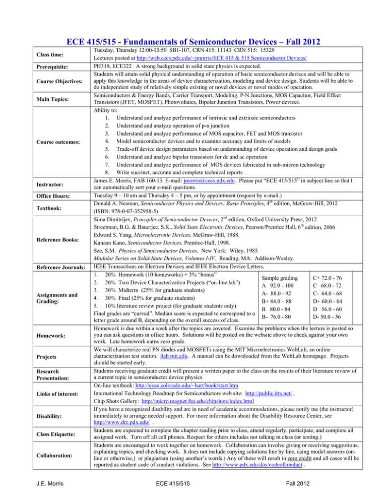
Tuesday, Thursday 12:00-13:50 SB1-107, CRN 415: 11143 CRN 515: 15329
Lectures posted at http://web.cecs.pdx.edu/~jmorris/ECE 415 & 515 Semiconductor Devices/
PH319, ECE322 A strong background in solid state physics is expected.
Students will attain solid physical understanding of operation of basic semiconductor devices and will be able to
apply this knowledge in the areas of device characterization, modeling and device design. Students will be able to
do independent study of relatively simple existing or novel devices or novel modes of operation.
Semiconductors & Energy Bands, Carrier Transport, Modeling, P-N Junctions, MOS Capacitor, Field Effect
Transistors (JFET, MOSFET), Photovoltaics, Bipolar Junction Transistors, Power devices.
Ability to:
1. Understand and analyze performance of intrinsic and extrinsic semiconductors
2. Understand and analyze operation of p-n junction
3. Understand and analyze performance of MOS capacitor, FET and MOS transistor
4. Model semiconductor devices and to examine accuracy and limits of models
5. Trade-off device design parameters based on understanding of device operation and design goals
6. Understand and analyze bipolar transistors for dc and ac operation
7. Understand and analyze performance of MOS devices fabricated in sub-micron technology
8. Write succinct, accurate and complete technical reports
James E. Morris, FAB 160-13. E-mail: jmorris@cecs.pdx.edu . Please put “ECE 415/515” in subject line so that I
can automatically sort your e-mail questions.
Tuesday 9 – 10 am and Thursday 4 – 5 pm, or by appointment (request by e-mail.)
Donald A. Neaman, Semiconductor Physics and Devices: Basic Principles, 4th edition, McGraw-Hill, 2012
(ISBN: 978-0-07-352958-5)
Sima Dimitrijev, Principles of Semiconductor Devices, 2nd edition, Oxford University Press, 2012
Streetman, B.G. & Banerjee, S.K., Solid State Electronic Devices, Pearson/Prentice Hall, 6th edition, 2006
Edward S. Yang, Microelectronic Devices, McGraw-Hill, 1988.
Kanaan Kano, Semiconductor Devices, Prentice-Hall, 1998.
Sze, S.M. Physics of Semiconductor Devices. New York: Wiley, 1985
Modular Series on Solid-State Devices, Volumes I-IV. Reading, MA: Addison-Wesley.
IEEE Transactions on Electron Devices and IEEE Electron Device Letters.
1. 20% Homework (10 homeworks) + 3% “bonus”
C+ 72.0 - 76
Sample grading
2. 20% Two Device Characterization Projects (“on-line lab”)
C 68.0 - 72
A 92.0 - 100
3. 30% Midterm (25% for graduate students)
C- 64.0 - 68
A- 88.0 - 92
4. 30% Final (25% for graduate students)
D+ 60.0 - 64
B+ 84.0 – 88
5. 10% literature review project (for graduate students only)
D 56.0 - 60
B 80.0 - 84
Final grades are “curved”. Median score is expected to correspond to a
D- 50.0 - 56
B- 76.0 - 80
letter grade around B, depending on the overall success of class.
Homework is due within a week after the topics are covered. Examine the problems when the lecture is posted so
you can ask questions in office hours. Solutions will be posted on the website above to check against your own
work. Late homework earns zero grade.
We will characterize real PN diodes and MOSFETs using the MIT Microelectronics WebLab, an online
characterization test station. ilab.mit.edu. A manual can be downloaded from the WebLab homepage. Projects
should be started early.
Students receiving graduate credit will present a written paper to the class on the results of their literature review of
a current topic in semiconductor device physics.
On-line textbook: http://ecee.colorado.edu/~bart/book/start.htm
International Technology Roadmap for Semiconductors web site: http://public.itrs.net/ ,
Chip Shots Gallery: http://micro.magnet.fsu.edu/chipshots/index.html
If you have a recognized disability and are in need of academic accommodations, please notify me (the instructor)
immediately to arrange needed support. For more information about the Disability Resource Center, see
http://www.drc.pdx.edu/ .
Students are expected to complete the chapter reading prior to class, attend regularly, participate, and complete all
assigned work. Turn off all cell phones. Respect for others includes not talking in class (or texting.)
Students are encouraged to work together on homework. Collaboration can involve giving or receiving suggestions,
explaining topics, and checking work. It does not include copying solutions line by line, using model answers (online or otherwise,) or plagiarism (using another’s words.) Any of these will result in zero credit and all cases will be
reported as student code of conduct violations. See http://www.pdx.edu/dos/codeofconduct .
ECE 415/515
Fall 2012
ECE 415/515 Schedule: Fall 2012 J.E. Morris (for planning purposes)
1
2
3
4
5
6
7
8
9
10
Day
Date
Reading
Topics or Tests
Homework & projects due
Tues
9/25
Ch 1 & 2
Course introduction; history of semiconductors;
review Ch 1 (crystals) & Ch 2 (quantum mech)
Thur
9/27
Ch 3.1 - 3
Semiconductors: Energy Bands
Tues
10/2
Ch 3.4 – 5
Ch 4.1 - 2
Semiconductors: Density of states, Fermi levels
Thur
10/4
Ch 4.3 - 6
Semiconductors: Extrinsic semiconductors
Tues
10/9
Ch 5
Semiconductors: Transport phenomena
Thur
10/11
Ch 6
Semiconductors: Non-equilibrium (excess carriers)
Tues
10/16
Ch 7
P-N Junctions: Equilibrium, bias
Thur
10/18
Ch 8
P-N Junctions: Currents, breakdown, transients &
ac (project)
Tues
10/23*
Ch 9
P-N Junctions: Metal-semiconductor/heterojunctions
HW4 (Ch 7 & 8) (2pts)
Thur
10/25*
Ch 10.1 - 2
MOSFET: MOS capacitor
PN diode project #1 due
Tues
10/30
Ch 10.3
MOSFET: MOSFET operation & characteristics
HW5 (Ch 9 & 10.1-10.2) (2pts)
Thur
11/1*
Ch 10.4
Ch 11.1
MOSFET: Frequency limits, (project), non-ideal,
sub-threshold
Tues
11/6
Ch 11.2 - 5
MOSFETs: Substrate bias, scaling, short channel, etc
Thur
11/8
Tues
11/13
Ch 12.1 - 3
BJTs: Operation, minority carrier, CB
HW7 (Ch 11.2-11.5) (1 pt)
Thur
11/15
Ch 12.4 - 8
BJTs: Non-ideal, models, switching
MOSFET project #2 due
Tues
11/20
Ch 15.4 - 6
Power:, BJT, MOSFET, 4-layer devices
HW8 (Ch 12) (2 pts)
Thur
11/22
Tues
11/27
Thur
Thu
HW1 (Ch 1, 2, 3.1-3.3) (2pts)
HW2 (Ch 3.4-3.5, 4.1-4.6) (2pts)
HW3 (Ch 5 & 6) (2pts)
HW6 (Ch 10.3-10.4, 11.1) (2pts)
MID-TERM EXAM: Chapters 1 - 9.
Thanksgiving Holiday
Ch 14.1 - 5
Optical: Solar cells, detectors, luminescence, LEDs
HW9 (Ch 15) (1 pt)
11/29
Graduate Project reports (oral with ppt slides)
HW10 (Ch 14) (1 pt)
12/6
FINAL EXAM: 10:15-12:05
MOSFETS, BJTS (Ch. 10-127) ETC (14.1-5, 15.5-6)
ECE515 graduate literature
project due 5 pm Friday 11/30
All course components must be completed satisfactorily, even if late. (Bonus 3 pts if all 10 HW’s submitted and non-zero)
* Lectures given by Prof C_W Nam.
J.E. Morris
ECE 415/515
Fall 2012


