PoS(SKADS 2009)053
advertisement
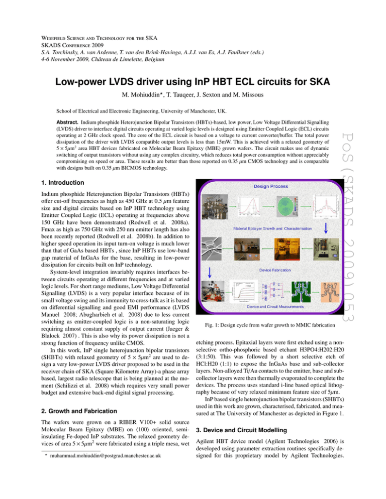
W S T SKA SKADS C 2009 S.A. Torchinsky, A. van Ardenne, T. van den Brink-Havinga, A.J.J. van Es, A.J. Faulkner (eds.) 4-6 November 2009, Château de Limelette, Belgium Low-power LVDS driver using InP HBT ECL circuits for SKA M. Mohiuddin? , T. Tauqeer, J. Sexton and M. Missous School of Electrical and Electronic Engineering, University of Manchester, UK. Abstract. Indium phosphide Heterojunction Bipolar Transistors (HBTs)-based, low power, Low Voltage Differential Signalling 1. Introduction Indium phosphide Heterojunction Bipolar Transistors (HBTs) offer cut-off frequencies as high as 450 GHz at 0.5 µm feature size and digital circuits based on InP HBT technology using Emitter Coupled Logic (ECL) operating at frequencies above 150 GHz have been demonstrated (Rodwell et al. 2008a). Fmax as high as 750 GHz with 250 nm emitter length has also been recently reported (Rodwell et al. 2008b). In addition to higher speed operation its input turn-on voltage is much lower than that of GaAs based HBTs , since InP HBTs use low-band gap material of InGaAs for the base, resulting in low-power dissipation for circuits built on InP technology. System-level integration invariably requires interfaces between circuits operating at different frequencies and at varied logic levels. For short range mediums, Low Voltage Differential Signalling (LVDS) is a very popular interface because of its small voltage swing and its immunity to cross-talk as it is based on differential signalling and good EMI performance (LVDS Manuel 2008; Abugharbieh et al. 2008) due to less current switching as emitter-coupled logic is a non-saturating logic requiring almost constant supply of output current (Jaeger & Blalock 2007) . This is also why its power dissipation is not a strong function of frequency unlike CMOS. In this work, InP single heterojunction bipolar transistors (SHBTs) with relaxed geometry of 5 × 5µm2 are used to design a very low-power LVDS driver proposed to be used in the receiver chain of SKA (Square Kilometre Array)-a phase array based, largest radio telescope that is being planned at the moment (Schilizzi et al. 2008) which requires very small power budget and extensive back-end digital signal processing. 2. Growth and Fabrication The wafers were grown on a RIBER V100+ solid source Molecular Beam Epitaxy (MBE) on h100i oriented, semiinsulating Fe-doped InP substrates. The relaxed geometry devices of area 5 × 5µm2 were fabricated using a triple mesa, wet ? muhammad.mohiuddin@postgrad.manchester.ac.uk PoS(SKADS 2009)053 (LVDS) driver to interface digital circuits operating at varied logic levels is designed using Emitter Coupled Logic (ECL) circuits operating at 2 GHz clock speed. The core of the ECL circuit is based on a voltage to current converter/buffer. The total power dissipation of the driver with LVDS compatible output levels is less than 15mW. This is achieved with a relaxed geometry of 5 × 5µm2 area HBT devices fabricated on Molecular Beam Epitaxy (MBE) grown wafers. The circuit makes use of dynamic switching of output transistors without using any complex circuitry, which reduces total power consumption without appreciably compromising on speed or area. These results are better than those reported on 0.35 µm CMOS technology and is comparable with designs built on 0.35 µm BICMOS technology. Fig. 1: Design cycle from wafer growth to MMIC fabrication etching process. Epitaxial layers were first etched using a nonselective ortho-phosphoric based etchant H3PO4:H202:H20 (3:1:50). This was followed by a short selective etch of HCl:H20 (1:1) to expose the InGaAs base and sub-collector layers. Non-alloyed Ti/Au contacts to the emitter, base and subcollector layers were then thermally evaporated to complete the devices. The process uses standard i-line based optical lithography because of very relaxed minimum feature size of 5µm. InP based single heterojunction bipolar transistors (SHBTs) used in this work are grown, characterised, fabricated, and measured at The University of Manchester as depicted in Figure 1. 3. Device and Circuit Modelling Agilent HBT device model (Agilent Technologies 2006) is developed using parameter extraction routines specifically designed for this proprietary model by Agilent Technologies. 312 M. Mohiuddin et al.: Low-power LVDS driver using InP HBT ECL circuits Fig. 2: LVDS driver with voltage to current converter. This non-linear, parametric model is based on the University of California, San Diego (UCSD) model (UCSD High Speed Devices Group 2000) which takes into account Kirk effect, velocity modulation effect, large knee voltage and other typical features of III-V HBTs. The circuit implementation of LVDS driver comprises two additional output transistors (encircled in Figure 2) than the conventional ECL stage. These additional criss-cross connected transistors are used to switch off current between the differential output circuits. Dynamic switching off of the output transistors without using any extra circuitry conserves considerable power (Abugharbieh et al. 2008), which in our designs was up to 20% reducing total power dissipation from 19 mW to less than 15 mW. Tail current for the differential pairs are provided using Wilson current mirror configuration to improve the output impedance of the basic current mirror design. Emitter resistors are used to reduce the temperature sensitivity of the circuit by offsetting the reduction in the turn-on voltage of the transistors as the temperature goes up. Voltage to current translators are used at the output stage to meet stringent load termination requirements of the LVDS standard. ECL input as shown in Figure 3 is the simulated random data which is fed to a simple master-slave D-latch stage (not shown). This stage gives input to the LVDS driver, which translates ECL levels to LVDS compatible levels as described below and as shown in Figure 3. LVDS standard requires the following typical output values: Voltage swing of 250 to 400 mV Offset voltage of 1.2 ± 0.2V Termination resistor of 100 Ohm differential 4. Conclusion In this work, a complete low voltage differential signalling (LVDS) driver is designed and simulated to work with ECL circuits operating at 2 GHz clock speed. The total power dissipation of the driver complete driver circuit is less than 15 mW. The driver is designed to interface Analogue to Digital PoS(SKADS 2009)053 Fig. 3: LVDS driver input and output waveforms Converter (ADC) with emitter coupled logic levels to the backend digital signal processing block of a radio telescope receiver chain through its built-in LVDS receiver. This power consumption is lower than that of designs reported using 0.35µm CMOS technology and is comparable with designs built with 0.35µm BICMOS technology. This reported InP HBT design has the added advantage of compatibility with the mainstream high speed InP technology. References M. J. W. Rodwell, M. Le, and B. Brar, “InP bipolar ICs: Scaling roadmaps, frequency limits, manufacturable technologies,” Proceedings of the Ieee, vol. 96, pp. 271-286, 2008. M. Rodwell, E. Lobisser, M. Wistey, V. Jain, A. Baraskar, E. Lind, J. Koo, Z. Griffith, J. Hacker, M. Urteaga, D. Mensa, R. Pierson, and B. Brar, “THz Bipolar Transistor Circuits: Technical Feasibility, Technology Development, Integrated Circuit Results,” 2008 Ieee Csic Symposium, pp. 1-3, 2008. “LVDS owner’s manual, Design guide,” 2008. K. Abugharbieh, J. Mohan, D. Varadarajan, I. Duzevik, and S. Krishnan, “An ultra low power 10 Gbps LVDS output driver,” Proceedings of the 2008 Bipolar/Bicmos Circuits and Technology Meeting, pp. 5-8, 2008. R. C. Jaeger and T. N. Blalock, Microelectronic circuit design. New York ; London: McGraw-Hill Higher Education, 2007. R. T. Schilizzi, P. E. F. Dewdney, and T. J. W. Lazio, “The Square Kilometre Array” in Ground-based and Airborne Telescopes II Marseille, France: SPIE, 2008. Agilent Technologies, 2006, “Agilent HBT Model,” in Nonlinear Devices Manual “HBT Model Equations. rev9.001a 3/2000” San Deigo: http: //hbt.ucsd.edu/, 2000.

