PE42524
Document Category: Product Specification
UltraCMOS® SPDT RF Switch, 10 MHz–40 GHz
Features
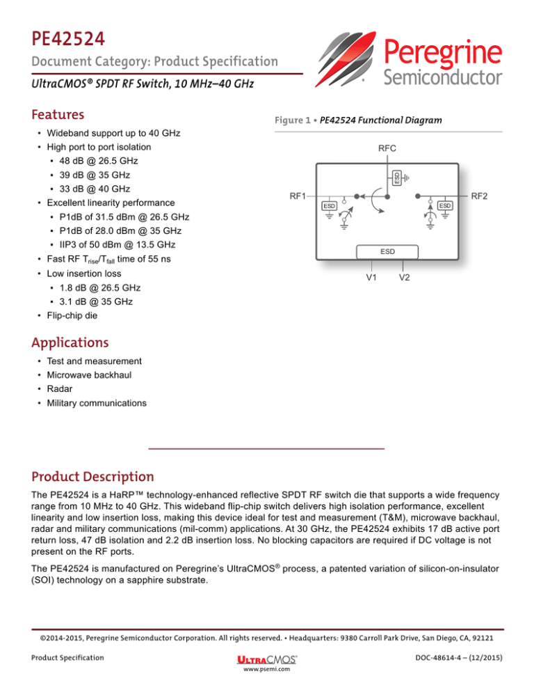
Figure 1 • PE42524 Functional Diagram
• Wideband support up to 40 GHz
• High port to port isolation
RFC
▪ 48 dB @ 26.5 GHz
▪ 39 dB @ 35 GHz
▪ 33 dB @ 40 GHz
• Excellent linearity performance
RF1
RF2
▪ P1dB of 31.5 dBm @ 26.5 GHz
▪ P1dB of 28.0 dBm @ 35 GHz
▪ IIP3 of 50 dBm @ 13.5 GHz
ESD
• Fast RF Trise/Tfall time of 55 ns
• Low insertion loss
V1
V2
▪ 1.8 dB @ 26.5 GHz
▪ 3.1 dB @ 35 GHz
• Flip-chip die
Applications
• Test and measurement
• Microwave backhaul
• Radar
• Military communications
Product Description
The PE42524 is a HaRP™ technology-enhanced reflective SPDT RF switch die that supports a wide frequency
range from 10 MHz to 40 GHz. This wideband flip-chip switch delivers high isolation performance, excellent
linearity and low insertion loss, making this device ideal for test and measurement (T&M), microwave backhaul,
radar and military communications (mil-comm) applications. At 30 GHz, the PE42524 exhibits 17 dB active port
return loss, 47 dB isolation and 2.2 dB insertion loss. No blocking capacitors are required if DC voltage is not
present on the RF ports.
The PE42524 is manufactured on Peregrine’s UltraCMOS® process, a patented variation of silicon-on-insulator
(SOI) technology on a sapphire substrate.
©2014-2015, Peregrine Semiconductor Corporation. All rights reserved. • Headquarters: 9380 Carroll Park Drive, San Diego, CA, 92121
Product Specification
DOC-48614-4 – (12/2015)
www.psemi.com
PE42524
SPDT RF Switch
Peregrine’s HaRP technology enhancements deliver high linearity and excellent harmonics performance. It is an
innovative feature of the UltraCMOS process, offering the performance of GaAs with the economy and
integration of conventional CMOS.
Absolute Maximum Ratings
Exceeding absolute maximum ratings listed in Table 1 may cause permanent damage. Operation should be
restricted to the limits in Table 2. Operation between operating range maximum and absolute maximum for
extended periods may reduce reliability.
ESD Precautions
When handling this UltraCMOS device, observe the same precautions as with any other ESD-sensitive devices.
Although this device contains circuitry to protect it from damage due to ESD, precautions should be taken to
avoid exceeding the rating specified in Table 1.
Latch-up Immunity
Unlike conventional CMOS devices, UltraCMOS devices are immune to latch-up.
Table 1 • Absolute Maximum Ratings for PE42524
Parameter/Condition
Min
Max
Unit
Control voltage (V1, V2)
–3.5
3.5
V
Fig. 2
dBm
+150
°C
2000
V
RF input power (RFC–RFX, 50Ω)
Storage temperature range
–65
ESD voltage HBM, all pins(*)
Note: * Human body model (MIL-STD883 Method 3015).
Page 2
DOC-48614-4 – (12/2015)
www.psemi.com
PE42524
SPDT RF Switch
Recommended Operating Conditions
Table 2 lists the recommended operating conditions for PE42524. Devices should not be operated outside the
recommended operating conditions listed below.
Table 2 • Recommended Operating Condition for PE42524
Parameter
Min
Typ
Max
Unit
Control high (V1, V2)
3.1
3.3
3.5
V
Control low (V1, V2)
–3.5
–3.3
–3.1
V
Control current
2
nA
RF input power, CW (RFC–RFX)(1)
Fig. 2
dBm
RF input power, pulsed (RFC–RFX)(2)
Fig. 2
dBm
+85
°C
Operating temperature range
–40
+25
Notes:
1) 100% duty cycle, all bands, 50Ω.
2) Pulsed, 5% duty cycle of 4620 μs period, 50Ω.
Electrical Specifications
Table 3 provides the PE42524 key electrical specifications @ 25 °C, V1 = +3.3V, V2 = –3.3V or V1 = –3.3V, V2
= +3.3V (ZS = ZL = 50Ω), unless otherwise specified.
Table 3 • PE42524 Electrical Specifications
Parameter
Path
Condition
Typ
10
MHz
Operation frequency
Insertion loss
Min
RFC–RFX
10 MHz
10 MHz–7.5 GHz
7.5–10 GHz
10–13.5 GHz
13.5–18 GHz
18–20 GHz
20–26.5 GHz
26.5–30 GHz
30–35 GHz
35–40 GHz
DOC-48614-4 – (12/2015)
0.6
1.0
1.1
1.3
1.4
1.4
1.8
2.2
3.1
5.5
Max
Unit
40
GHz
As
shown
0.85
1.30
1.50
1.65
1.75
1.75
2.20
2.70
4.10
—
dB
dB
dB
dB
dB
dB
dB
dB
dB
dB
Page 3
www.psemi.com
PE42524
SPDT RF Switch
Table 3 • PE42524 Electrical Specifications
Parameter
Path
Condition
Min
Typ
Max
Unit
74
60
58
51
50
49
44
43
35
28
84
64
65
58
53
52
48
47
39
33
dB
dB
dB
dB
dB
dB
dB
dB
dB
dB
All paths
10 MHz
10 MHz–7.5 GHz
7.5–10 GHz
10–13.5 GHz
13.5–18 GHz
18–20 GHz
20–26.5 GHz
26.5–30 GHz
30–35 GHz
35–40 GHz
RFC–RFX
10 MHz
10 MHz–7.5 GHz
7.5–10 GHz
10–13.5 GHz
13.5–18 GHz
18–20 GHz
20–26.5 GHz
26.5–30 GHz
30–35 GHz
35–40 GHz
25
16
15
17
21
21
18
17
14
6
dB
dB
dB
dB
dB
dB
dB
dB
dB
dB
RFC–RFX
10 MHz
10 MHZ–7.5 GHz
7.5–10 GHz
10–13.5 GHz
13.5–18 GHz
18–20 GHz
20–26.5 GHz
26.5–30 GHz
30–35 GHz
35–40 GHz
25
18
19
26
29
23
31
30
16
7
dB
dB
dB
dB
dB
dB
dB
dB
dB
dB
RFC–RFX
+25 dBm output power, 1 GHz
+25 dBm output power, 6.5 GHz
+25 dBm output power, 15 GHz
88
84
>89(1)
dBc
dBc
dBc
Input 1dB compression
point(2)
10 MHz–40 GHz
Fig. 2
dBm
Input IP3
10–100 MHz
1–2 GHz
6–10 GHz
10–13.5 GHz
48
50
52
50
dBm
dBm
dBm
dBm
Video feedthrough(3)
DC measurement
3.5
mVPP
RF Trise/Tfall
10%/90% RF
55
ns
Settling time
50% CTRL to 0.05 dB final value
Isolation
Return loss (active port)
Return loss (RFC port)
2nd harmonic, 2fo rejection
Page 4
0.84
1.13
μs
DOC-48614-4 – (12/2015)
www.psemi.com
PE42524
SPDT RF Switch
Table 3 • PE42524 Electrical Specifications
Parameter
Path
Switching time
Condition
Min
50% CTRL to 90% or 10% RF
Typ
Max
Unit
225
304
ns
Notes:
1) Test system limited.
2) The input 1dB compression point is a linearity figure of merit. Refer to Table 2 for the RF input power (50Ω).
3) Measured with a 3.5 ns rise time, –3.3 / +3.3V pulse and 500 MHz bandwidth.
Control Logic
Table 4 • Truth Table for PE42524
Table 4 provides the control logic truth table for the
PE42524. States 2 and 3 are used in normal switching
operations.
V1
V2
RF1
RF2
State
–3.3V
–3.3V
OFF
OFF
1
–3.3V
+3.3V
OFF
ON
2
+3.3V
–3.3V
ON
OFF
3
+3.3V
+3.3V
ON
ON
4
Figure 2 • Power De-rating Curve (10 MHz–40 GHz) @ 25 °C and 85 °C Ambient (50Ω)
P1 dB Compression / Abs. Max. RF Input Power @ 25°C & 85°C Ambient
Max. RF Input Power, Pulsed @ 25°C & 85°C Ambient
Input Power (dBm)
Max. RF Input Power, CW @ 25°C & 85°C Ambient
34
33
32
31
30
29
28
27
26
25
24
23
22
21
20
0.01
5.01
10.01
15.01
20.01
25.01
30.01
35.01
40.01
Frequency (GHz)
DOC-48614-4 – (12/2015)
Page 5
www.psemi.com
PE42524
SPDT RF Switch
Typical Performance Data
Figure 3–Figure 12 show the typical performance data @ 25 °C, V1 = +3.3V, V2 = –3.3V, unless otherwise
specified.
Figure 3 • Insertion Loss vs Temperature (RFC–RFX)
−40°C
+25°C
+85°C
0
Insertion Loss (dB)
−2
−4
−6
−8
−10
0
5
10
15
20
25
30
35
40
30
35
40
Frequency (GHz)
Figure 4 • Insertion Loss vs V1/V2 (RFC–RFX)
+3.1V/−3.1V
+3.3V/−3.3V
0
Insertion Loss (dB)
−2
−4
−6
−8
−10
0
5
10
15
20
25
Frequency (GHz)
Page 6
DOC-48614-4 – (12/2015)
www.psemi.com
PE42524
SPDT RF Switch
Figure 5 • RFC Port Return Loss vs Temperature
−40°C
+25°C
+85°C
Return Loss (dB)
−10
−15
−20
−25
−30
−35
−40
0
5
10
15
20
25
30
35
40
30
35
40
Frequency (GHz)
Figure 6 • RFC Port Return Loss vs V1/V2
+3.1V/−3.1V
+3.3V/−3.3V
Return Loss (dB)
−10
−15
−20
−25
−30
−35
−40
0
5
10
15
20
25
Frequency (GHz)
DOC-48614-4 – (12/2015)
Page 7
www.psemi.com
PE42524
SPDT RF Switch
Figure 7 • Active Port Return Loss vs Temperature
−40°C
+25°C
+85°C
Return Loss (dB)
−10
−15
−20
−25
−30
−35
−40
0
5
10
15
20
25
30
35
40
30
35
40
Frequency (GHz)
Figure 8 • Active Port Return Loss vs V1/V2
+3.1V/−3.1V
+3.3V/−3.3V
Return Loss (dB)
−10
−15
−20
−25
−30
−35
−40
0
5
10
15
20
25
Frequency (GHz)
Page 8
DOC-48614-4 – (12/2015)
www.psemi.com
PE42524
SPDT RF Switch
Figure 9 • Isolation vs Temperature (RFX–RFX)
−40°C
+25°C
+85°C
0
−10
Isolation (dB)
−20
−30
−40
−50
−60
−70
−80
−90
0
5
10
15
20
25
30
35
40
30
35
40
Frequency (GHz)
Figure 10 • Isolation vs V1/V2 (RFX–RFX)
+3.1V/−3.1V
+3.3V/−3.3V
0
−10
Isolation (dB)
−20
−30
−40
−50
−60
−70
−80
−90
0
5
10
15
20
25
Frequency (GHz)
DOC-48614-4 – (12/2015)
Page 9
www.psemi.com
PE42524
SPDT RF Switch
Figure 11 • Isolation vs Temperature (RFC–RFX)
−40°C
+25°C
+85°C
0
−10
Isolation (dB)
−20
−30
−40
−50
−60
−70
−80
−90
0
5
10
15
20
25
30
35
40
30
35
40
Frequency (GHz)
Figure 12 • Isolation vs V1/V2 (RFC–RFX)
+3.1V/−3.1V
+3.3V/−3.3V
0
−10
Isolation (dB)
−20
−30
−40
−50
−60
−70
−80
−90
0
5
10
15
20
25
Frequency (GHz)
Page 10
DOC-48614-4 – (12/2015)
www.psemi.com
PE42524
SPDT RF Switch
Recommended Evaluation Setup
The PE42524 s-parameter data and input 1dB compression point from 22–40 GHz (Table 3 and Figure 3–
Figure 12) were taken using grounded co-planar waveguide (CPWG) on the alumina substrate (shown in
Figure 13) and RF probes.
The PE42524 2nd harmonic, 2fo rejection, input 1dB compression point below 18 GHz, input IP3 measurements, settling time and switching time (Table 3) were taken on a PCB using 2.92 mm connectors.
Bypass capacitors are not required.
PCB using 2.92 mm connectors.pacitors are not required
Figure 13 • Alumina Substrate Board for PE42524
Alumina substrate board
Thickness: 0.01 in.
εR = 9.9
RFC
RF2
PE42524
DIE
V1
RF1
V2
DOC-48614-4 – (12/2015)
Page 11
www.psemi.com
PE42524
SPDT RF Switch
Pin Configuration
Table 5 • Pin Descriptions for PE42524
This section provides pin information for the
PE42524. Figure 14 shows the pin configuration of
this device. Table 5 provides a description for each
pin.
Figure 14 • Pin Configuration (Bumps Up) for PE42524
9
GND
GND
RFC
Pin
Name
1, 2, 5, 6,
8–10, 12–
14, 16–19
GND
Ground
7
RF1
RF port 1
11
RFC
RF common port
15
RF2
RF port 2
3
V1
Control input 1
4
V2
Control input 2
13
GND
10
Pin No.
GND
12
Description
11
GND
GND
8
14
GND
GND
18
16
RF1
7
GND
5
RF2
GND
GND
19
17
15
GND
GND
6
2
V2
V1
4
3
GND
1
Page 12
DOC-48614-4 – (12/2015)
www.psemi.com
PE42524
SPDT RF Switch
Die Mechanical Specifications
This section provides the die mechanical specifications for the PE42524.
Table 6 • Mechanical Specifications for PE42524
Parameter
Min
Typ
Max
Unit
Die size, singulated (x, y)
2466 × 2120
2486 × 2140
2516 × 2170
μm
180
200
220
μm
Wafer thickness
Wafer size
150
Bump pitch
500
Bump height
72.5
Bump diameter
UBM diameter
Including excess sapphire,
max. tolerance = –20 / +30 μm
mm
μm
85
97.75
90
μm
μm
110
85
Test Condition
95
DOC-48614-4 – (12/2015)
μm
Page 13
www.psemi.com
PE42524
SPDT RF Switch
Table 7 • Pin Coordinates for PE42524(*)
Figure 15 • Pin Layout for PE42524(1)(2)
Pin Center (μm)
Pin Name
X
9
Y
1
GND
1128.5
–958.5
2
GND
731.5
–646.5
3
V1
253.5
–958.5
4
V2
–253.5
–958.5
GND
GND
13
GND
RFC
10
GND
12
11
GND
5
GND
–1128.5
–958.5
6
GND
–731.5
–646.5
7
RF1
–785.5
–121.5
8
GND
–931.5
363.5
9
GND
–1091.5
913.5
10
GND
–503.5
753.5
11
RFC
0
629
12
GND
503.5
753.5
13
GND
1091.5
913.5
14
GND
931.5
363.5
15
RF2
785.5
–121.5
16
GND
253.5
183.5
17
GND
253.5
–326.5
18
GND
–253.5
183.5
19
GND
–253.5
–326.5
GND
8
GND
GND
18
16
14
RF1
7
GND
5
2140 μm (−20 / +30 μm)
Pin #
RF2
GND
GND
19
17
15
GND
GND
6
2
V2
V1
4
3
GND
1
2486 μm (−20 / +30 μm)
Notes:
1) Drawings are not drawn to scale.
2) Singulated die size shown, bump side up.
Note: * All pin locations originate from the die center and refer to the
center of the pin.
Page 14
DOC-48614-4 – (12/2015)
www.psemi.com
PE42524
SPDT RF Switch
Tape and Reel Specification
This section provides the tape and reel specifications for the PE42524.
Figure 16 • Tape and Reel Specifications for PE42524
ø1.50 ± 0.1
0.20 ± 0.05
2.00 ± 0.05
4.00 ± 0.1
4.00 ± 0.1
1.75 ± 0.1
3.50 ± 0.05
Bo
8.00 ± 0.1
ø0.50 ± 0.05
Ko
Ao
Pocket Nominal Tolerance
Ao
2.35
± 0.05
Bo
2.66
± 0.05
Ko
0.395
± 0.05
Pin 1
Notes:
Not Drawn to Scale
Dimensions are in millimeters
Maximum cavity angle 5 degrees
Bumped die are oriented active side down
Device Orientation in Tape
DOC-48614-4 – (12/2015)
Page 15
www.psemi.com
PE42524
SPDT RF Switch
Ordering Information
Table 8 lists the available ordering code for the PE42524 as well as shipping method.
Table 8 • Order Code for PE42524
Order Code
Description
Packaging
Shipping Method
PE42524A–X
PE42524 SPDT RF switch
Die on tape and reel
500 die / T&R
Document Categories
Advance Information
Product Brief
The product is in a formative or design stage. The datasheet contains
design target specifications for product development. Specifications
and features may change in any manner without notice.
This document contains a shortened version of the datasheet. For the
full datasheet, contact sales@psemi.com.
Preliminary Specification
Not Recommended for New Designs (NRND)
This product is in production but is not recommended for new designs.
The datasheet contains preliminary data. Additional data may be added
at a later date. Peregrine reserves the right to change specifications at
any time without notice in order to supply the best possible product.
Product Specification
The datasheet contains final data. In the event Peregrine decides to
change the specifications, Peregrine will notify customers of the
intended changes by issuing a CNF (Customer Notification Form).
End of Life (EOL)
This product is currently going through the EOL process. It has a
specific last-time buy date.
Obsolete
This product is discontinued. Orders are no longer accepted for this
product.
Sales Contact
For additional information, contact Sales at sales@psemi.com.
Disclaimers
The information in this document is believed to be reliable. However, Peregrine assumes no liability for the use of this information. Use shall be
entirely at the user’s own risk. No patent rights or licenses to any circuits described in this document are implied or granted to any third party.
Peregrine’s products are not designed or intended for use in devices or systems intended for surgical implant, or in other applications intended to
support or sustain life, or in any application in which the failure of the Peregrine product could create a situation in which personal injury or death
might occur. Peregrine assumes no liability for damages, including consequential or incidental damages, arising out of the use of its products in
such applications.
Patent Statement
Peregrine products are protected under one or more of the following U.S. patents: patents.psemi.com
Copyright and Trademark
©2014-2015, Peregrine Semiconductor Corporation. All rights reserved. The Peregrine name, logo, UTSi and UltraCMOS are registered trademarks and HaRP, MultiSwitch and DuNE are trademarks of Peregrine Semiconductor Corp.
Product Specification
www.psemi.com
DOC-48614-4 – (12/2015)
