αRD2520/C5B, αRD2522/C5B
Data Sheet
High bandwidth, High Slew Rate,
Uncompensated, High Input Impedance,
Operational Amplifiers
Operational amplifiers αRD2520 delivering an
unsurpassed combination of specifications for slew rate,
bandwidth and settling time. These amplifiers are
controlled at close loop gains greater than 3 without
external compensation. In addition, these high
performance components also provide low offset
current and high input impedance.
100 V/µs slew rate and 200 ns (0.1 %) settling time of
these amplifiers make them ideal components for pulse
amplification and data acquisition designs. These devices
are valuable components for RF and video circuitry
requiring up to 20 MHz gain bandwidth and 2 MHz
power bandwidth. For accurate signal conditioning
designs the αRD2520’s superior dynamic specifications
are complemented by 25nA offset current, 50MΩ input
impedance and offset trim capability.
These amplifiers have been developed and certified as
HiRel and high RadHard components for airspace and
defense equipment.
December 16, 2011
RDm061D
Features
•
•
•
•
•
•
•
•
•
•
High slew rate. . . . . . . . . . . . . . . 100 V/µs
Fast Settling . . . . . . . . . . . . . . . . 500 ns
Full Power Bandwidth. . . . . . . . . 2 MHz
Gain Bandwidth. . . . . . . . . . . . . . 20 MHz
High Input Impedance. . . . . . . . . 50 MΩ
Low Offset Current. . . . . . . . . . . 25 nA
High RadHard. . . . . . . . . . . . . . . 105 rad
Compensation Pin for Unity Gain Capability
Balance pins
RoHS Compliant
Applications
•
•
•
•
•
Data Acquisition Systems
RF Amplifiers
Video Amplifiers
Signal Generators
Pulse Amplification
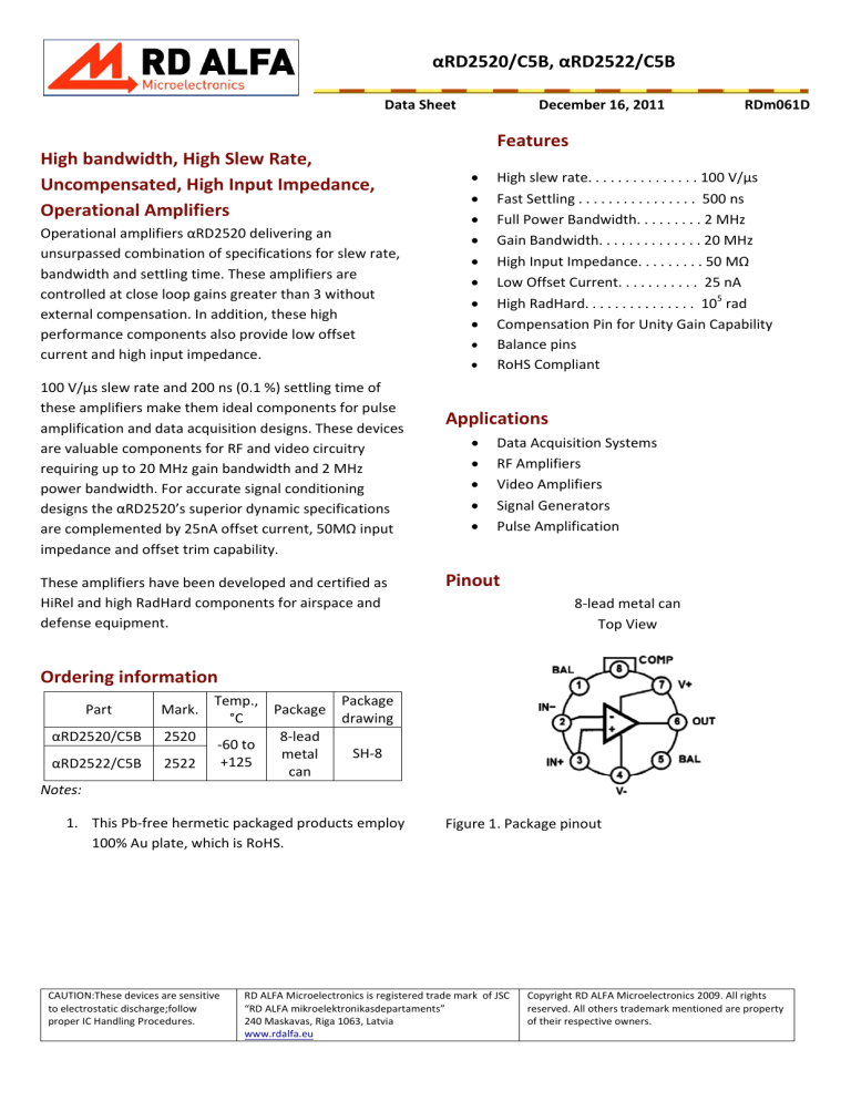
Pinout
8‐lead metal can
Top View
Ordering information
Part
Mark.
αRD2520/C5B
2520
αRD2522/C5B
2522
Temp.,
Package
Package
°C
drawing
8‐lead
‐60 to
SH‐8
metal
+125
can
Notes:
1. This Pb‐free hermetic packaged products employ
100% Au plate, which is RoHS.
CAUTION:These devices are sensitive
to electrostatic discharge;follow
proper IC Handling Procedures.
Figure 1. Package pinout
RD ALFA Microelectronics is registered trade mark of JSC
“RD ALFA mikroelektronikasdepartaments”
240 Maskavas, Riga 1063, Latvia
www.rdalfa.eu
Copyright RD ALFA Microelectronics 2009. All rights
reserved. All others trademark mentioned are property
of their respective owners.
αRD2520/C5B, αRD2520/C5B
Operation Condition
Absolute Maximum Ratings
SupplyVoltage(BetweenV+andV‐Terminals)..36 V
Differential Input Voltages. . . . . . . . .. . . . . . . 10 V
Common Mode Input Voltage (note 3) . . . . . . . . 10 V
OutputCurrent. . . . . .. . . . . . . . . . .. . . . . . . . . . 10 mA
Total Power (from ‐60 °C to 108 °C) . . . . . . . . . . 350 mW
Total Power (above 108°C) – see fig.20
Short circuit at the output . . . . . . . . . . . . . . . . . . 10 s
Notes:
2. While of the same time of above mentioned
supply voltage and output current not more 1 h
3. Common mode Input Voltage is determined in
accordance with fig.11
Temperature range ‐60 °C to +125 °C
Operating Supply Voltage ± 15 V ±10 %
RL ≥2 kΩ
Thermal Information
Thermal Resistance (typical)
θJA = 170 °C/W (note 4)
θJC = 85 °C/W (note 5)
Maximum junction temperature +170 °C
Lead temperature (soldering 3 s) 350 °C
Notes:
4. θJA is measured with component on an
evaluation PC board in free air
5. For θJC “case temp” location is the center of
metal can
Electrical Specifications
VSUPPLY = ± 15 V ± 10 %
αRD2520/C5B
Parameter
Temp., °C
Min
(note 6)
25
+125
‐60
‐60 to 25
25 to +125
25
+125
‐60
25
+125
‐60
‐60 to 25
25 to +125
25
+125
‐60
25
+125
‐60
25
‐
‐
‐
‐
‐
‐
‐
‐
‐
‐
‐
Typ
Max
(note 6)
4.0
5.3
5.3
13
13
100
175
175
14
24
24
225
225
‐
‐
‐
‐
‐
‐
50
9
12
12
30
30
225
450
450
30
60
60
500
500
‐
‐
‐
‐10
‐10
‐10
‐
αRD2522/C5B
Min
Max
Typ
(note 6)
(note 6)
Units
Input Characteristics
Offset Voltage
(note 8)
Offset Voltage Drift (note 8)
Average bias current (note 8)
Offset Current
(note 8)
Offset Current Drift (note 8)
Maximum Common Mode
Voltage (note 9)
Minimum Common Mode
Voltage (note 9)
Input Resistance (note 7)
2
+10
+10
+10
‐
‐
‐
‐
‐
‐
‐
‐
‐
‐
‐
‐
‐
‐
‐
‐
‐
+10
+10
+10
‐
‐
‐
‐
4.0
5.3
5.3
13
13
125
270
270
22
45
45
225
225
‐
‐
‐
‐
‐
‐
50
RDm061D 12/16/11
9
12
12
50
30
300
600
600
50
100
100
1000
500
‐
‐
‐
‐10
‐10
‐10
‐
mV
µV/°C
nA
nA
pA/°C
V
V
MΩ
αRD2520/C5B, αRD2520/C5B
Parameter
Temp., °C
αRD2520/C5B
Min
Max
Typ
(note 6)
(note 6)
αRD2522/C5B
Min
Max
Typ
(note 6)
(note 6)
Units
Transfer characteristics
Large Signal Voltage Gain
(note 9, 14)
Common Mode Rejection
Ratio (note 8)
Gain Bandwidth (note 7, 15)
Minimum Stable Gain
Output Characteristics
Maximum Output Voltage
(note 9)
Minimum Output Voltage
(note 9)
Output Current (note 13)
Full Power Bandwidth (note
13, 16)
Transient Response
Rise Time (note 9, 10, 11, 17)
Overshoot (note 9, 10, 17)
Slew rate (note 9, 10, 12, 19)
Settling Time (note 8, 18)
Power Supply Characteristics
Supply Current
Power Supply Rejection Ratio
(note 11)
25
+125
‐60
25
+125
‐60
25
25
8
7
7
82
80
80
10
3
11.8
9.1
9.1
88
88
88
20
‐
‐
‐
‐
‐
‐
‐
‐
‐
7.5
5.5
5.5
82
80
80
10
3
10
7.1
7.1
88
88
88
20
‐
‐
‐
‐
‐
‐
‐
‐
‐
25
+125
‐60
25
+125
‐60
25
9.5
9
9
‐
‐
‐
10
12
10.5
10.5
‐12
‐10.5
‐10.5
12.5
‐
‐
‐
‐9.5
‐9
‐9
‐
9.5
9.0
9.0
‐
‐
‐
10
12
10.5
10.5
‐12
‐10.5
‐10.5
12.4
‐
‐
‐
‐9.5
‐9
‐9
‐
mA
25
1.5
2.0
‐
1.5
2.0
‐
MHz
25
25
25
25
‐
‐
80
‐
25
10
100
200
50
25
‐
‐
‐
‐
70
‐
25
10
100
200
50
25
‐
‐
ns
%
V/µs
ns
25
+125
‐60
25
+125
‐60
‐
‐
‐
80
80
80
6.0
6.5
6.5
90
90
90
7.0
7.5
7.5
‐
‐
‐
‐
‐
‐
74
74
74
6.0
6.5
6.5
90
90
90
7.0
7.5
7.5
‐
‐
‐
kV/V
dB
MHz
V/V
V
V
mA
dB
Notes:
6. Parameters with Max and Min limits are 100 %
tested.
7. Parameter is controlled via design or process
parameters and is not directly tested at final
production. This parameter is lab characterized
upon initial design release, or upon design
changes. This parameter is guaranteed by
characterization based upon data from multiple
production runs which reflect lot to lot and
within lot variation.
8. RL = 10 kΩ
9. RL = 2 kΩ
10. CL = 50 pF
3
11.
12.
13.
14.
15.
16.
VOUT = ±200 mV
VOUT = ±5 V
VOUT = ±10 V
VCM = ±10 V
AV≥ 10
Full Power Bandwidth guaranteed based on slew
rate measurement using
FPBW = Slew Rate/2πVOUT MAX
17. See figure 3 and 4
18. See figure 2 and 5
19. See figure 2 and 4
RDm061D 12/16/11
αRD2520/C5B, αRD2520/C5B
Test Circuits and Waveforms
Figure 2. Slew rate and settling time
Figure 5. Settling time test circuit
Figure 3.Transient response
Figure 6. Suggested offset voltage adjustment and
compensation hook‐up
Figure 4. Slew rate and trensient response test circuit
4
RDm061D 12/16/11
αRD2520/C5B, αRD2520/C5B
Schematic Diagram
Figure 7.αRD2520,αRD2522 schematic diagram
5
RDm061D 12/16/11
αRD2520/C5B, αRD2520/C5B
Typical Application
Figure8showsaCompensationCircuitforaninvertingunity
gainamplifier.Thecircuitwastestedforfunctionalitywith
supplyvoltagesfrom±5 Vto±15V,andtheperformanceas
testedwas:SlewRate≈100V/µs;Bandwidth≈7 MHz;and
SettlingTime(0.1%)≈500ns.Figure9illustratestheamplifier’s
frequencyresponse,anditisimportanttonotethatcapacitanc
e atpin8mustbeminimizedformaximumbandwidth.
GAIN(dB)
InvertingUnityGainCircuit
Figure 9. Frequency response for inverting unity gain
circuit
Figure 8.Inverting unity gain circuit
6
RDm061D 12/16/11
αRD2520/C5B, αRD2520/C5B
Typical Performance Curve
Figure 10. Offset voltage vs temperature
Figure 11. Bias current vs temperature
Figure 12. Offset current vs temperature
Figure 13. Open loop gain vs temperature
7
RDm061D 12/16/11
αRD2520/C5B, αRD2520/C5B
Figure 15. Supply current vs supply voltage
Figure 14. Maximum and minimum output voltage vs
supply voltage
Figure 16. Normalized settling time vs supply voltage
8
Figure 17. . Normalized slew rate and bandwidth vs
supply voltage
RDm061D 12/16/11
αRD2520/C5B, αRD2520/C5B
Figure 19. Output voltage swing vs frequency
Figure 18. Frequency response
Figure 20. Open loop frequency response for various
capacitor values on the comp pin
9
RDm061D 12/16/11
αRD2520/C5B, αRD2520/C5B
Die Characteristics
Die dimensions:
1.8x1.7± 0.1 mm,
71x67 ± 4 mils.
Wafer thickness 0.46± 0.02 mm,
18 ± 1 mils.
Metallization:
type: Al, 1% Si,thickness: 1.4 ± 0.1 µm
Glassivation:
type: Phosphosilicate glass (PSG)
PSG thickness 1.2 ±0.2µm.
Worst case current density:
8∙104 A/cm2.
Substrate potential(Powered Up):
Unbiased.
Transistor count:
30.
Process:
Bipolar epitaxial.
Metallization Mask layout
Figure 21.Metallization layout
10
RDm061D 12/16/11
αRD2520/C5B, αRD2520/C5B
Metal Can Package
Notes:
20. (All leads) Øb applies between L1 and L2. Øb1
applies between L2 and 0.500 from the
reference plane. Diameter is uncontrolled in L1
and beyond 0.500 from the reference plane.
21. Measured from maximum diameter of the
product.
22. α is the basic spacing from the centerline of the
tab to terminal 1 and β is the basic spacing of
each lead or lead position (N ‐1 places) from a,
looking at the bottom of the package.
23. N is the maximum number of terminal positions.
24. Controlling dimension: millimeter.
SF‐8
8‐lead metal can package
Millimeters
Symbol
MIN
MAX
A
6.00
6.22
Øb
0.41
0.48
Øb1
0.41
0.53
Øb2
0.41
0.61
ØD
9.09
9.19
ØD1
8.23
8.43
Øe
0.200
e1
0.100
F
0.33
0.43
k
0.69
0.86
k1
0.69
1.14
L
13.0
14.0
L1
‐
1.27
L2
6.35
6.85
Q
0.5
‐
α
45°
β
45°
N
8
Inches
MIN
MAX
0.236
0.244
0.016
0.019
0.016
0.021
0.016
0.024
0.335
0.375
0.305
0.335
5.08
2.54
0.013
0.017
0.027
0.034
0.027
0.045
0.512
0.552
‐
0.05
0.250
0.270
0.02
‐
45°
45°
8
Note
‐
13
13
‐
‐
‐
‐
‐
‐
‐
14
13
13
13
‐
15
15
16
Figure 22. Package
All RD ALFA Microelectronics semiconductor products are manufactured, assembled and tested under ISO9001 quality
systems certification.
RD ALFA Microelectronics products are sold by description only. RD ALFA Microelectronics reserves the right to make changes in circuit design and/or specifications at
any time without notice. Accordingly, the reader is cautioned to verify that data sheets are current before placing orders. Information furnished by RD ALFA
Microelectronics is believed to be accurate and reliable. However, no responsibility is assumed by RD ALFA Microelectronics or its subsidiaries for its use; nor for any
infringements of patents or other rights of third parties which may result from its use. No license is granted by implication or otherwise under any patent or patent
rights of RD ALFA Microelectronics or its subsidiaries.
For information regarding RD ALFA Microelectronics and its products, see web site http://www.rdalfa.eu.
11
RDm061D 12/16/11


