Two-dimensional to three-dimensional tunneling in InAs/AlSb/GaSb
advertisement
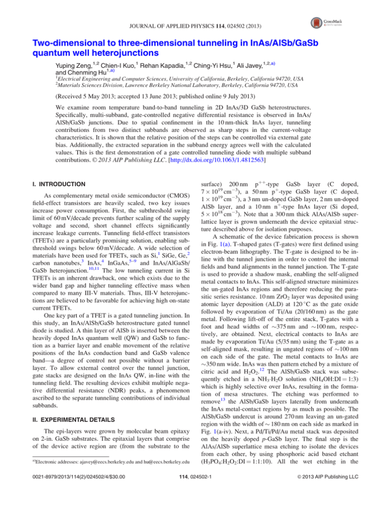
JOURNAL OF APPLIED PHYSICS 114, 024502 (2013) Two-dimensional to three-dimensional tunneling in InAs/AlSb/GaSb quantum well heterojunctions Yuping Zeng,1,2 Chien-I Kuo,1 Rehan Kapadia,1,2 Ching-Yi Hsu,1 Ali Javey,1,2,a) and Chenming Hu1,a) 1 Electrical Engineering and Computer Sciences, University of California, Berkeley, California 94720, USA Materials Sciences Division, Lawrence Berkeley National Laboratory, Berkeley, California 94720, USA 2 (Received 5 May 2013; accepted 13 June 2013; published online 9 July 2013) We examine room temperature band-to-band tunneling in 2D InAs/3D GaSb heterostructures. Specifically, multi-subband, gate-controlled negative differential resistance is observed in InAs/ AlSb/GaSb junctions. Due to spatial confinement in the 10 nm-thick InAs layer, tunneling contributions from two distinct subbands are observed as sharp steps in the current-voltage characteristics. It is shown that the relative position of the steps can be controlled via external gate bias. Additionally, the extracted separation in the subband energy agrees well with the calculated values. This is the first demonstration of a gate controlled tunneling diode with multiple subband C 2013 AIP Publishing LLC. [http://dx.doi.org/10.1063/1.4812563] contributions. V I. INTRODUCTION As complementary metal oxide semiconductor (CMOS) field-effect transistors are heavily scaled, two key issues increase power consumption. First, the subthreshold swing limit of 60 mV/decade prevents further scaling of the supply voltage and second, short channel effects significantly increase leakage currents. Tunneling field-effect transistors (TFETs) are a particularly promising solution, enabling subthreshold swings below 60 mV/decade. A wide selection of materials have been used for TFETs, such as Si,1 SiGe, Ge,2 carbon nanotubes,3 InAs,4 InGaAs,5–9 and InAs/AlGaSb/ GaSb heterojunction.10,11 The low tunneling current in Si TFETs is an inherent drawback, one which exists due to the wider band gap and higher tunneling effective mass when compared to many III-V materials. Thus, III-V heterojunctions are believed to be favorable for achieving high on-state current TFETs. One key part of a TFET is a gated tunneling junction. In this study, an InAs/AlSb/GaSb heterostructure gated tunnel diode is studied. A thin layer of AlSb is inserted between the heavily doped InAs quantum well (QW) and GaSb to function as a barrier layer and enable movement of the relative positions of the InAs conduction band and GaSb valence band—a degree of control not possible without a barrier layer. To allow external control over the tunnel junction, gate stacks are designed on the InAs QW, in-line with the tunneling field. The resulting devices exhibit multiple negative differential resistance (NDR) peaks, a phenomenon ascribed to the separate tunneling contributions of individual subbands. II. EXPERIMENTAL DETAILS The epi-layers were grown by molecular beam epitaxy on 2-in. GaSb substrates. The epitaxial layers that comprise of the device active region are (from the substrate to the a) Electronic addresses: ajavey@eecs.berkeley.edu and hu@eecs.berkeley.edu 0021-8979/2013/114(2)/024502/4/$30.00 surface) 200 nm pþþ-type GaSb layer (C doped, 7 1019 cm3), a 50 nm pþ-type GaSb layer (C doped, 1 1019 cm3), a 3 nm un-doped GaSb layer, 2 nm un-doped AlSb layer, and a 10 nm nþ-type InAs layer (Si doped, 5 1018 cm3). Note that a 300 nm thick AlAs/AlSb superlattice layer is grown underneath the device epitaxial structure described above for isolation purposes. A schematic of the device fabrication process is shown in Fig. 1(a). T-shaped gates (T-gates) were first defined using electron-beam lithography. The T-gate is designed to be inline with the tunnel junction in order to control the internal fields and band alignments in the tunnel junction. The T-gate is used to provide a shadow mask, enabling the self-aligned metal contacts to InAs. This self-aligned structure minimizes the un-gated InAs regions and therefore reducing the parasitic series resistance. 10 nm ZrO2 layer was deposited using atomic layer deposition (ALD) at 120 C as the gate oxide followed by evaporation of Ti/Au (20/160 nm) as the gate metal. Following lift-off of the entire stack, T-gates with a foot and head widths of 375 nm and 100 nm, respectively, are obtained. Next, electrical contacts to InAs are made by evaporation Ti/Au (5/35 nm) using the T-gate as a self-aligned mask, resulting in ungated regions of 100 nm on each side of the gate. The metal contacts to InAs are 350 nm wide. InAs was then pattern etched by a mixture of citric acid and H2O2.12 The AlSb/GaSb stack was subsequently etched in a NH3H2O solution (NH4OH:DI ¼ 1:3) which is highly selective over InAs, resulting in the formation of mesa structures. The etching was performed to remove13 the AlSb/GaSb layers laterally from underneath the InAs metal-contact regions by as much as possible. The AlSb/GaSb undercut is around 270 nm leaving an un-gated region with the width of 180 nm on each side as marked in Fig. 1(a-iv). Next, a Pd/Ti/Pd/Au metal stack was deposited on the heavily doped p-GaSb layer. The final step is the AlAs/AlSb superlattice mesa etching to isolate the devices from each other, by using phosphoric acid based etchant (H3PO4:H2O2:DI ¼ 1:1:10). All the wet etching in the 114, 024502-1 C 2013 AIP Publishing LLC V 024502-2 Zeng et al. experiment was carried out at room temperature. The scanning electron microscopy (SEM) images of a fabricated device are shown in Fig. 1(b). III. RESULTS AND DISCUSSION Electrical characterization of the devices was carried out at room temperature with an Agilent 4155 semiconductor parameter analyzer (Fig. 2(a)). Figure 2(b) shows measured current, I, as a function of the applied tunnel diode voltage, VTD, at different gate bias, VG, for a representative device. Interestingly, two distinct NDR peaks in the I - VTD characteristics are visible, exhibiting steepness of 25 mV/decade and 6 mV/decade, at VG ¼ 0 V. Analysis shows that these steps correspond to tunneling between the two lowest electron subbands of the InAs QW and the bulk GaSb valence band, illustrating the characteristics of tunneling in a 2-D to 3-D junction. The InAs QW here is defined by the 10 nm thick InAs that is sandwiched between a 10 nm ZrO2 layer on top and 2 nm AlSb layer on the bottom, which gives rise to the 2D subband formation.14 Furthermore, by changing VG, a shift in the voltage positions of the peaks is observed, demonstrating the gate control over the device. By varying the gate bias, the carrier concentration in the InAs can be controlled, moving the position of the Fermi energy level with respect to the subband edges and subsequently changing the VTD at which tunneling occurs. Additionally, in FIG. 1. (a) Fabrication process flow. (b) Representative SEM images of a device after fabrication. The magnified image depicts the elevated InAs QW floor, which was designed to isolate the InAs QW from the GaSb substrate. J. Appl. Phys. 114, 024502 (2013) the forward bias region, the diffusion current dominates at high voltages, while in the reverse bias region, the expected tunnel current is observed. Note that given the T-shaped gate geometry used here, the gate fields will be different for the regions directly beneath the foot and the head of the gate. However, the gate-dependence of the static I-V characteristics is dominated by the regions directly under the gate foot given the stronger gate field in those regions.15 I-VG at a fixed VTD was also measured. Figure 2(c) shows an I-VG curve of the same device when VTD is fixed at 0.45 V. Analogous to the I-VTD curves, two steps in the current are observed. These steps are due to the change in the Fermi level with respect to the InAs subband edges, enabling control over the number of subbands contributing to tunnel current at a given junction voltage. The VG positions at which the current rises agree well with Fig. 2(b). By taking the derivative of current as a function of the applied voltage (either VTD or VG) in Figs. 2(b) and 2(c), FIG. 2. (a) Device schematic showing the configuration of the applied voltages. (b) The measured current as a function of the tunnel diode voltage (VTD) when the gate bias VG is swept from 0.4 V to 1.2 V in 0.4 V steps. (c) The measured current as a function of the gate bias at a fixed VTD of 0.45 V. The device active area is 0.375 24 lm2. 024502-3 Zeng et al. J. Appl. Phys. 114, 024502 (2013) peak positions (T1 and T2) arising from the two lowest InAs subbands can be obtained from the experimental data. Here, the gate coupling ratio, which is the ratio of the peak position separation DVTD from Fig. 2(b) over the peak position separation DVG from Fig. 2(c), is approximately 23%. While already high, the gate coupling may be further improved in the future by device epilayer structure design optimization and the use of thinner gate dielectric layers. At VG < 0.4 V, the current becomes gate independent. We attribute this current to the un-gated junction regions as marked in Fig. 1(a-iv) beneath the metal contacts. In the future, a more controlled etch of the GaSb/AlSb layers under the metal contact areas is needed to further reduce this ungated tunneling path. Similar multiple peak negative differential resistance behavior was also observed in Refs. 16 and 17; additionally, in this work, the peak position dependence on gate bias is demonstrated for the first time. In order to gain better insight into the above multi-peak NDR behavior, a cross-sectional band alignment of the device is depicted in Fig. 3(a). The effect of the applied VTD is also qualitatively shown. The 10 nm thick InAs is structurally confined and thus exhibits step-wise 2-D density of states. The energy spacing of the subbands in the InAs layer and the spacing between the NDR peaks can be simulated by using Nextnano simulation tool. In Nextnano, by specifying quantum well region and including 1-band-schroedinger equations, energy band diagram and the subband energy levels can be both simulated. The experimental NDR peak positions (T1, T2) and spacing (T2-T1) obtained from I-VTD curves as a function of the gate bias are plotted in Fig. 3(b). The corrected peak position spacing after taking into account the voltage drop across the estimated series resistance in the device is also shown. From the I-VTD curve, the series resistance of the tunneling diode can be estimated to be 51 X by taking the slope of the curve in the region where diffusion current dominates. By subtracting the voltage drop due to this series resistance from the total applied VTD, the peak spacings at each gate bias can be corrected as shown in Fig. 3(b). The corrected experimental and calculated peak spacings match well as shown in Fig. 3(b). This provides strong support that the observed multipeak NDR is due to tunneling between InAs 1st (E1) and 2nd (E2) subbands and the GaSb valence band. Note that the sharpness of the steps is enhanced when series resistance is large. Similar effect of series resistance on I-V characteristics has also been reported in Ref. 18. To further analyze our results, the analytical model shown below was fit to the experimental data. The total current in the tunnel diode can be expressed in the following equation: qVTD 1Þ; (1) Idif f usion ¼ I0 ðexp KT FIG. 3. (a) Qualitative band alignment of the 2D/3D tunnel diode. (b) The measured peak positions (T1, T2) and separations (T2-T1) as a function of V G. Itunnel ¼ C ð Evp Ecn vi T DOSc DOSv ðFn Fp ÞdE; (3) DOSc þ DOSv where vi represents the injected velocity in the ith subband of InAs, T represents the tunneling probability, DOSc and DOSv stand for the density of states of conduction band of InAs and valence band of GaSb, and F represents the Fermi-Dirac distribution functions. n and p represent electrons and holes, respectively. Additionally, the following assumptions were utilized: (1) the tunneling probability is calculated via the WKB approximation; (2) electron velocity was given by the z-component of the momentum in the InAs quantum well qffiffiffiffiffi i (vi ¼ 2E m , where Ei is the energy of the ith bound state); where I0 is assumed to be 1011 A Idiode ¼ Itunnel þ Idif f usion ; with the tunneling component calculated via19 (2) FIG. 4. Measured (red) and simulated (black) I-V curves of a gated diode at VG ¼ 0 V. 024502-4 Zeng et al. (3) the InAs DOS is 2-D with effective mass me ¼ 0.032m0, the GaSb DOS is 3-D with effective mass mh ¼ 0.34m0. EC(InAs) ¼ 4.92 eV, EV(GaSb) ¼ 4.06 eV, E2-EC ¼ 0.31 eV, E2E1 ¼ 0.09 eV, C ¼ 6.7 1032 were applied in this calculation. The joint density of states DOSc DOSv =ðDOSc þ DOSv Þ was used, as it enables capture of the key features in a 2-D to 3-D tunneling junction. The sharpness of the drop in the experimental behavior is affected by the series resistance.18 To account for the series resistance in the simulation, a load line analysis model was used on the calculated I-V curves similar to Ref. 18. The calculated I-V is shown in Fig. 4, which is in good agreement with the experimental data, further highlighting the tunneling current in a 2-D to 3-D junction. IV. CONCLUSIONS In summary, negative differential resistance with multiple peaks from InAs/AlSb/GaSb system is experimentally demonstrated and theoretically analyzed. Critically, the results show that the peak positions can be controlled by an external gate bias demonstrating that this structure is an excellent candidate for future TFET devices. Furthermore, it is shown that the observed voltage spacings between the current peaks fit well with calculated subband spacings of the 2D InAs, and that the observed I-V behavior may be fit with a simple tunnel diode model. Finally, the observation of gate-controlled tunneling between a quantum well and a bulk semiconductors is of great importance, as it allows TFETs with junctions of various dimensionalities to be explored.20 ACKNOWLEDGMENTS This work was supported by the Center for Energy Efficient Electronics Science (NSF Award 0939514). J. Appl. Phys. 114, 024502 (2013) 1 W. Y. Choi, B. G. Park, J. D. Lee, and T. J. K. Liu, IEEE Electron Device Lett. 28, 743 (2007). 2 T. Krishnamohan, D. Kim, S. Raghunathan, and K. Saraswat, Tech. Dig. Int. Electron Devices Meet. 2008, 947–949. 3 J. Appenzeller, Y. M. Lin, J. Knoch, and P. Avouris, Phys. Rev. Lett. 93, 196805 (2004). 4 A. C. Ford, C. W. Yeung, S. Chuang, H. S. Kim, E. Plis, S. Krishna, C. Hu, and A. Javey, Appl. Phys. Lett. 98, 113105 (2011). 5 S. Mookerjea, D. Mohata, R. Krishnan, J. Singh, A. Vallett, A. Ali, T. Mayer, V. Narayanan, D. Schlom, A. Liu, and S. Datta, Tech. Dig. - Int. Electron Devices Meet. 2009, 949–951. 6 G. Dewey, B. Chu-Kung, J. Boardman, J. M. Fastenau, J. Kavalieros, R. Kotlyar, W. K. Liu, D. Lubyshev, M. Metz, N. Mukherjee, P. Oakey, R. Pillarisetty, M. Radosavljevic, H. W. Then, and R. Chau, Tech. Dig. - Int. Electron Devices Meet. 2011, 785–788. 7 H. Zhao, Y. Chen, Y. Wang, F. Zhou, F. Xue, and J. Lee, IEEE Electron Device Lett. 31, 1392 (2010). 8 S. Mookerjea, D. Mohata, T. Mayer, V. Narayanan, and S. Datta, IEEE Electron Device Lett. 31, 564 (2010). 9 B. Rajamohanan, D. Mohata, A. Ali, and S. Datta, Appl. Phys. Lett. 102, 092105 (2013). 10 G. L. Zhou, R. Li, T. Vasen, M. Qi, S. Chae, Y. Lu, Q. Zhang, H. Zhu, J. M. Kuo, T. Kosel, M. Wistey, P. Fay, A. Seabaugh, and H. L. Xing, IEEE Trans. Electron Devices 2012, 777–780. 11 R. Li, Y. Q. Lu, G. L. Zhou, Q. M. Liu, S. D. Chae, T. Vasen, W. S. Hwang, Q. Zhang, P. Fay, T. Kosel, M. Wistey, H. L. Xing, and A. Seabaugh, IEEE Electron Device Lett. 33, 363 (2012). 12 G. C. Desalvo, R. Kaspi, and C. A. Bozada, J. Electrochem. Soc. 141, 3526 (1994). 13 A. R. Clawson, Mater. Sci. Eng. 31, 1 (2001). 14 K. Takei, H. Fang, S. B. Kumar, R. Kapadia, Q. Gao, M. Madsen, H. S. Kim, C. H. Liu, Y. L. Chueh, E. Plis, S. Krishna, H. A. Bechtel, J. Guo, and A. Javey, Nano Lett. 11, 5008 (2011). 15 J. Mateos, T. Gonzalez, D. Pardo, V. Hoel, and A. Cappy, Semicond. Sci. Technol. 14, 864 (1999). 16 Y. H. Wang, M. H. Liu, M. P. Houng, J. F. Chen, and A. Y. Cho, IEEE Trans. Electron Devices 41, 1734 (1994). 17 S. M. Sze and K. K. Ng, Physics of Semiconductor Devices, 3rd ed. (Wiley, John & Sons, 2007), pp. 457. 18 J. M. A. Gilman and A. G. O’Neill, J. Appl. Phys. 74, 351 (1993). 19 J. M. A. Gilman and A. G. O’Neill, J. Appl. Phys. 71, 2741 (1992). 20 S. Agarwal, “Reinventing the PN junction: Dimensionality effects on tunneling switches,” Ph.D. dissertation (University of California at Berkeley, 2012).
