851010
1-to-10, Differential HCSL Fanout Buffer
Datasheet
General Description
Features
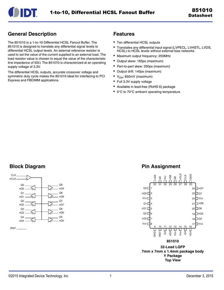
The 851010 is a 1-to-10 Differential HCSL Fanout Buffer. The
851010 is designed to translate any differential signal levels to
differential HCSL output levels. An external reference resistor is
used to set the value of the current supplied to an external load. The
load resistor value is chosen to equal the value of the characteristic
line impedance of 50. The 851010 is characterized at an operating
supply voltage of 3.3V.
•
•
Ten differential HCSL outputs
•
•
•
•
•
•
•
•
Maximum output frequency: 250MHz
The differential HCSL outputs, accurate crossover voltage and
symmetric duty cycle makes the 851010 ideal for interfacing to PCI
Express and FBDIMM applications.
Block Diagram
Translates any differential input signal (LVPECL, LVHSTL, LVDS,
HCSL) to HCSL levels without external bias networks
Output skew: 165ps (maximum)
Part-to-part skew: 250ps (maximum)
Output drift: 140ps (maximum)
VOH: 850mV (maximum)
Full 3.3V supply voltage
Available in lead-free (RoHS 6) package
0°C to 70°C ambient operating temperature
Q4
nQ4
Q5
nQ5
IREF
CLK
GND
nCLK
Q8
nQ8
VDD
3
22
VDD
Q1
4
21
nQ6
nQ1
5
20
Q6
Q2
6
19
nQ5
nQ2
7
18
Q5
VDD
8
17
VDD
9
10 11 12 13 14 15 16
Q4
Q6
nQ6
Q7
nQ4
Q3
nQ3
23
VDD
Q7
nQ7
nQ7
2
VDD
Q2
nQ2
24
nQ0
Q3
Q8
nQ8
1
nQ3
Q1
nQ1
32 31 30 29 28 27 26 25
Q0
GND
Q9
nQ9
IREF
Q0
nQ0
VDD
nQ9
CLK
nCLK
Q9
Pin Assignment
851010
32-Lead LQFP
7mm x 7mm x 1.4mm package body
Y Package
Top View
©2015 Integrated Device Technology, Inc
1
December 3, 2015
851010 Datasheet
Table 1. Pin Descriptions
Number
Name
Type
Description
1, 2
Q0, nQ0
Output
Differential output pair. Differential HCSL interface levels.
3, 8, 13, 14,
17, 22, 30
VDD
Power
Positive supply pins.
4, 5
Q1, nQ1
Output
Differential output pair. Differential HCSL interface levels.
6, 7
Q2, nQ2
Output
Differential output pair. Differential HCSL interface levels.
9, 25
GND
Power
Power supply ground.
10
IREF
Input
Reference current input. Used to set the output current. Connect to 950 resistor to ground.
11, 12
Q3, nQ3
Output
Differential output pair. Differential HCSL interface levels.
15, 16
Q4, nQ4
Output
Differential output pair. Differential HCSL interface levels.
18, 19
Q5, nQ5
Output
Differential output pair. Differential HCSL interface levels.
20, 21
Q6, nQ6
Output
Differential output pair. Differential HCSL interface levels.
23, 24
Q7, nQ7
Output
Differential output pair. Differential HCSL interface levels.
26
CLK
Input
Non-inverting differential input.
27
nCLK
Input
Inverting differential clock input.
28, 29
Q8, nQ8
Output
Differential output pair. Differential HCSL interface levels.
31, 32
Q9, nQ9
Output
Differential output pair. Differential HCSL interface levels.
Output Driver Current
The 851010 outputs are HCSL differential current dr ive with
the current being set with a resistor from IREF to ground. For
a single load and a 50 pc board trace, the drive current would
typically be set with a RREF of 950 which products an IREF of 1.16mA.
The IREF is multiplied by a current mirror to an output drive of
12*1.16mA or 13.90mA. See Figure 1 for current mirror and output
drive details.
IREF
RREF
950Ω
RL
RL
Figure 1. HCSL Current Mirror and Output Drive
©2015 Integrated Device Technology, Inc
2
December 3, 2015
851010 Datasheet
Absolute Maximum Ratings
NOTE: Stresses beyond those listed under Absolute Maximum Ratings may cause permanent damage to the device.
These ratings are stress specifications only. Functional operation of product at these conditions or any conditions beyond
those listed in the DC Characteristics or AC Characteristics is not implied. Exposure to absolute maximum rating conditions for
extended periods may affect product reliability.
Item
Rating
Supply Voltage, VDD
4.6V
Inputs, VI
-0.5V to VDD + 0.5V
Outputs, IO
-0.5V to VDD + 0.5V
Package Thermal Impedance, JA
65.7°C/W (0 mps)
Storage Temperature, TSTG
-65C to 150C
DC Electrical Characteristics
Table 2A. Power Supply DC Characteristics, VDD = 3.3V±5%, TA = 0°C to 70°C
Symbol
Parameter
Test Conditions
VDD
Core Supply Voltage
IDD
Power Supply Current; NOTE 1
Minimum
Typical
Maximum
Units
3.135
3.3
3.465
V
105
mA
NOTE 1: Measured using 200MHz input frequency.
Table 2B. Differential DC Characteristics, VDD = 3.3V±5%, TA = 0°C to 70°C
Symbol
Parameter
Test Conditions
IIH
Input
High Current
CLK, nCLK
IIL
Input
Low Current
CLK, nCLK
VPP
Peak-to-Peak Voltage; NOTE 1
VCMR
Common Mode Input Voltage;
NOTE 1, 2
Minimum
Typical
Maximum
Units
VDD = VIN = 3.465V
5
µA
VDD = 3.465V, VIN = 0V
5
µA
0.15
1.3
V
GND + 0.5
VDD – 0.85
V
NOTE 1: VIL should not be less than -0.3V.
NOTE 2: Common mode input voltage is defined as VIH.
©2015 Integrated Device Technology, Inc
3
December 3, 2015
851010 Datasheet
AC Electrical Characteristics
Table 3. HCSL AC Characteristics, VDD = 3.3V±5%, TA = 0°C to 70°C
Symbol
Parameter
Test Conditions
Minimum
fMAX
Output Frequency
tPD
Propagation Delay, NOTE 1
Measured on at VOX
1.5
tsk(o)
Output Skew; NOTE 2, 3
Measured on at VOX
tsk(pp)
Part-to-Part Skew; NOTE 3, 4
tjit
Buffer Additive Phase Jitter, RMS
tsk(drift)
Output Drift; NOTE 5
VMAX
Absolute Max Output Voltage; NOTE 6
ƒ 150MHz
VMIN
Absolute Min Output Voltage; NOTE 6
ƒ 150MHz
VCROSS
Absolute Crossing Voltage;
NOTE 7, 8, 9
VCROSS
Total Variation of VCROSS over all
edges; NOTE 7, 8, 10
tR / tF
Rise/Fall Edge Rate; NOTE 11, 12
odc
Output Duty Cycle; NOTE 13
CLK = 200MHz, Integration
Range: 12kHz – 30MHz
Typical
Maximum
Units
250
MHz
2.75
ns
165
ps
250
ps
0.24
ps
140
ps
500
850
mV
-150
150
mV
250
550
mV
140
mV
0.6
4.0
V/ns
47
53
%
NOTE: Electrical parameters are guaranteed over the specified ambient operating temperature range, which is established when the device is
mounted in a test socket with maintained transverse airflow greater than 500 lfpm. The device will meet specifications after thermal equilibrium
has been reached under these conditions.
NOTE: Current adjust set for VOH = 0.7V. Measurements refer to PCIEX outputs only.
NOTE: Characterized using an RREF value of 950 resistor.
NOTE 1: Measured from the differential input cross point to the differential output crossing point.
NOTE 2: Defined as skew between outputs at the same supply voltage and with equal load conditions. Measured at the differential output
cross point.
NOTE 3: This parameter is defined in accordance with JEDEC Standard 65.
NOTE 4: Defined as skew between outputs on different devices operating at the same supply voltage, same frequency, same temperature and
with equal load conditions. Using the same type of inputs on each device, the outputs are measured at the differential cross point.
NOTE 5: Output Drift is measured as the change in the time placement of the differential cross point for each output on a given device due to
a change in temperature and supply voltage. Measured at the differential cross point.
NOTE 6: Measurement using RREF = to 950, RLOAD = to 50.
NOTE 7: Measurement taken from single-ended waveform.
NOTE 8: Measured at crossing point where the instantaneous voltage value of the rising edge of Qx equals the falling edge of nQx.
See Parameter Measurement Information Section.
NOTE 9: Refers to the total variation from the lowest crossing point to the highest, regardless of which edge is crossing. Refers to all crossing
points for this measurement. See Parameter Measurement Information Section.
NOTE 10: Defined as the total variation of all crossing voltage of rising Qx and falling nQx. This is the maximum allowed variance in the
VCROSS for any particular system. See Parameter Measurement Information Section.
NOTE 11: Measurement taken from differential waveform.
NOTE 12: Measurement from -150mV to +150mV on the differential waveform (derived from Qx minus nQx). The signal must be monotonic
through the measurement region for rise and fall time. The 300mV measurement window is centered on the differential zero crossing.
NOTE 13: Assuming 50% input duty cycle. Data taken at ƒ 200MHz, unless otherwise specified.
©2015 Integrated Device Technology, Inc
4
December 3, 2015
851010 Datasheet
Parameter Measurement Information
3.3V±5%
VDD
SCOPE
50Ω
33Ω
VDD
49.9Ω
HCSL
2pF
HCSL
50Ω
33Ω
50Ω
VDD
Measurement
Point
50Ω
Measurement
Point
IREF
GND
GND
49.9Ω
950Ω
2pF
0V
This load condition is used for IDD,tsk(pp), tjit(Ø), tPD and tsk(o)
measurements.
HCSL Output Load AC Test Circuit
HCSL Output Load AC Test Circuit
VDD
nQx
Qx
nCLK
V
Cross Points
PP
V
CMR
nQy
CLK
Qy
GND
Differential Input Levels
nQx
Output Skew
Par t 1
nCLK
CLK
Qx
nQy
Par t 2
nQ[0:9]
Q[0:9]
Qy
tPD
tsk(pp)
Part-to-Part Skew
©2015 Integrated Device Technology, Inc
Propagation Delay
5
December 3, 2015
851010 Datasheet
Parameter Measurement Information, continued
Differential Measurement Points for Duty Cycle/Period
Single-ended Measurement Points for Absolute Cross
Point and Swing
Single-ended Measurement Points for Delta Cross Point
Differential Measurement Points for Rise/Fall Edge Rate
©2015 Integrated Device Technology, Inc
6
December 3, 2015
851010 Datasheet
Applications Information
Recommendations for Unused Output Pins
Outputs:
Differential Outputs
All unused differential outputs can be left floating. We recommend
that there is no trace attached. Both sides of the differential output
pair should either be left floating or terminated.
Wiring the Differential Input to Accept Single-Ended Levels
Figure 2 shows how a differential input can be wired to accept single
ended levels. The reference voltage VREF = VDD/2 is generated by
the bias resistors R1 and R2. The bypass capacitor (C1) is used to
help filter noise on the DC bias. This bias circuit should be located as
close to the input pin as possible. The ratio of R1 and R2 might need
to be adjusted to position the VREF in the center of the input voltage
swing. For example, if the input clock swing is 2.5V and VDD = 3.3V,
R1 and R2 value should be adjusted to set VREF at 1.25V. The values
below are for when both the single ended swing and VDD are at the
same voltage. This configuration requires that the sum of the output
impedance of the driver (Ro) and the series resistance (Rs) equals
the transmission line impedance. In addition, matched termination at
the input will attenuate the signal in half. This can be done in one of
two ways. First, R3 and R4 in parallel should equal the transmission
line impedance. For most 50 applications, R3 and R4 can be 100.
The values of the resistors can be increased to reduce the loading for
slower and weaker LVCMOS driver. When using single-ended
signaling, the noise rejection benefits of differential signaling are
reduced. Even though the differential input can handle full rail
LVCMOS signaling, it is recommended that the amplitude be
reduced. The datasheet specifies a lower differential amplitude,
however this only applies to differential signals. For single-ended
applications, the swing can be larger, however VIL cannot be less
than -0.3V and VIH cannot be more than VDD + 0.3V. Though some
of the recommended components might not be used, the pads
should be placed in the layout. They can be utilized for debugging
purposes. The datasheet specifications are characterized and
guaranteed by using a differential signal.
Figure 2. Recommended Schematic for Wiring a Differential Input to Accept Single-ended Levels
©2015 Integrated Device Technology, Inc
7
December 3, 2015
851010 Datasheet
Differential Clock Input Interface
with the vendor of the driver component to confirm the driver
termination requirements. For example in Figure 3A, the input
termination applies for IDT open emitter LVHSTL drivers. If you are
using an LVHSTL driver from another vendor, use their termination
recommendation.
The CLK/nCLK accepts HCSL, LVDS, LVPECL and SSTL and other
differential signals. Both differential signals must meet the VPP and
VCMR input requirements. Figures 3A to 3F show interface examples
for the CLK/nCLK input driven by the most common driver types. The
input interfaces suggested here are examples only. Please consult
3.3V
1.8V
Zo = 50Ω
CLK
Zo = 50Ω
nCLK
Differential
Input
LVHSTL
R1
50Ω
IDT
LVHSTL Driver
R2
50Ω
Figure 3B. CLK/nCLK Input Driven by a
3.3V LVPECL Driver
Figure 3A. CLK/nCLK Input Driven by an IDT
Open Emitter LVHSTL Driver
3.3V
3.3V
3.3V
R3
125
3.3V
R4
125
3.3V
Zo = 50Ω
Zo = 50Ω
CLK
CLK
R1
100
Zo = 50Ω
nCLK
Differential
Input
LVPECL
R1
84
R2
84
Figure 3C. CLK/nCLK Input Driven by a
3.3V LVPECL Driver
3.3V
nCLK
Zo = 50Ω
Differential
Input
LVDS
Figure 3D. CLK/nCLK Input Driven by a 3.3V LVDS Driver
2.5V
3.3V
3.3V
2.5V
R3
120
*R3
R4
120
Zo = 60Ω
CLK
CLK
Zo = 60Ω
nCLK
nCLK
HCSL
*R4
Differential
Input
SSTL
R1
120
Differential
Input
Figure 3F. CLK/nCLK Input Driven by an SSTL Driver
Figure 3E. CLK/nCLK Input Driven by a
3.3V HCSL Driver
©2015 Integrated Device Technology, Inc
R2
120
8
December 3, 2015
851010 Datasheet
Recommended Termination
Figure 4A is the recommended termination for applications which
require the receiver and driver to be on a separate PCB. All traces
should be 50 impedance.
Figure 4A. Recommended Termination
Figure 4B is the recommended termination for applications which
require a point to point connection and contain the driver and receiver
on the same PCB. All traces should all be 50 impedance.
Figure 4B. Recommended Termination
©2015 Integrated Device Technology, Inc
9
December 3, 2015
851010 Datasheet
Power Considerations
This section provides information on power dissipation and junction temperature for the 851010.
Equations and example calculations are also provided.
1.
Power Dissipation.
The total power dissipation for the 851010 is the sum of the core power plus the power dissipated in the load(s). The following is the power
dissipation for VDD = 3.3V + 5% = 3.465V, which gives worst case results.
•
Power (core)MAX = VDD_MAX * IDD_MAX = 3.465V * 105mA = 363.825mW
•
Power (outputs)MAX = 44.5mW/Loaded Output Pair
If all outputs are loaded, the total power is 10 * 44.5mW = 445mW
Total Power_MAX (3.465V, with all outputs switching) = 363.825mW + 445mW = 808.825mW
•
2. Junction Temperature.
Junction temperature, Tj, is the temperature at the junction of the bond wire and bond pad directly affects the reliability of the device. The
maximum recommended junction temperature is 125°C. Limiting the internal transistor junction temperature, Tj, to 125°C ensures that the bond
wire and bond pad temperature remains below 125°C.
The equation for Tj is as follows: Tj = JA * Pd_total + TA
Tj = Junction Temperature
JA = Junction-to-Ambient Thermal Resistance
Pd_total = Total Device Power Dissipation (example calculation is in section 1 above)
TA = Ambient Temperature
In order to calculate junction temperature, the appropriate junction-to-ambient thermal resistance JA must be used. Assuming no air flow and
a multi-layer board, the appropriate value is 65.7°C/W per Table 4 below.
Therefore, Tj for an ambient temperature of 70°C with all outputs switching is:
70°C + 0.809W * 65.7°C/W = 123.2°C. This is below the limit of 125°C.
This calculation is only an example. Tj will obviously vary depending on the number of loaded outputs, supply voltage, air flow and the type of
board (multi-layer).
Table 4. Thermal Resistance JA for 32 Lead LQFP, Forced Convection
JA by Velocity
Meters per Second
Multi-Layer PCB, JEDEC Standard Test Boards
©2015 Integrated Device Technology, Inc
0
1
2.5
65.7°C/W
55.9°C/W
52.4°C/W
10
December 3, 2015
851010 Datasheet
The purpose of this section is to calculate power dissipation on the IC per HCSL output pair.
HCSL output driver circuit and termination are shown in Figure 5.
VDD
IOUT = 17mA
➤
VOUT
RREF =
950Ω ± 1%
RL
50Ω
IC
Figure 5. HCSL Driver Circuit and Termination
HCSL is a current steering output which sources a maximum of 17mA of current per output. To calculate worst case on-chip power dissipation,
use the following equations which assume a 50 load to ground.
The highest power dissipation occurs when VDD_MAX.
Power
= (VDD_MAX – VOUT) * IOUT,
since VOUT – IOUT * RL
= (VDD_MAX – IOUT * RL) * IOUT
= (3.465V – 17mA * 50) * 17mA
Total Power Dissipation per output pair = 44.5mW
©2015 Integrated Device Technology, Inc
11
December 3, 2015
851010 Datasheet
Reliability Information
Table 5. JA vs. Air Flow Table for a 32 Lead LQFP
JA vs. Air Flow
Meters per Second
Multi-Layer PCB, JEDEC Standard Test Boards
0
1
2.5
65.7°C/W
55.9°C/W
52.4°C/W
Transistor Count
The transistor count for 851010 is: 843
©2015 Integrated Device Technology, Inc
12
December 3, 2015
851010 Datasheet
Package Outline and Package Dimensions
Package Outline - Y Suffix for 32 Lead LQFP
Table 6. Package Dimensions for 32 Lead LQFP
JEDEC Variation: BBA
All Dimensions in Millimeters
Symbol
Minimum
Nominal
Maximum
N
32
A
1.60
A1
0.05
0.15
A2
1.35
1.40
1.45
b
0.30
0.37
0.45
c
0.09
0.20
D&E
9.00 Basic
D1 & E1
7.00 Basic
D2 & E2
5.60 Ref.
e
0.80 Basic
L
0.45
0.60
0.75
0°
7°
ccc
0.10
Reference Document: JEDEC Publication 95, MS-026
©2015 Integrated Device Technology, Inc
13
December 3, 2015
851010 Datasheet
Ordering Information
Table 7. Ordering Information
Part/Order Number
851010AYLF
851010AYLFT
Marking
ICS851010AYL
ICS851010AYL
©2015 Integrated Device Technology, Inc
Package
Lead-Free, 32 Lead LQFP
Lead-Free, 32 Lead LQFP
14
Shipping Packaging
Tray
Tape & Reel
Temperature
0°C to 70°C
0°C to 70°C
December 3, 2015
851010 Datasheet
Revision History Sheet
Rev
Table
Page
T1
2
2
4
5
T3
A
7
10 -11
13
T7
A
14
Description of Change
Date
Pin Description Table, IREF description corrected 475ohm resistor to 950ohm.
Corrected Output Driver Current and diagram.
Added note, “Characterized using....”.
Added Propagation Delay diagram and corrected HCSL Output Load AC Test Circuit
diagram in Parameter Measurement Information section.
Updated Wiring the Differential Input to Accept Single-ended Levels.
Corrected power dissipation calculation and total power dissipation section. Corrected
HCSL Driver Circuit Termination diagram.
Updated Package Outline.
Converted datasheet format.
8/2/10
Ordering Information - removed leaded devices. Removed the Lead Free note and the
quantity (1000) in the shipping packaging field.
Updated datasheet format.
12/3/15
©2015 Integrated Device Technology, Inc
15
December 3, 2015
851010 Datasheet
Corporate Headquarters
Sales
Tech Support
6024 Silver Creek Valley Road
San Jose, CA 95138 USA
www.IDT.com
1-800-345-7015 or 408-284-8200
Fax: 408-284-2775
www.IDT.com/go/sales
www.idt.com/go/support
DISCLAIMER Integrated Device Technology, Inc. (IDT) reserves the right to modify the products and/or specifications described herein at any time, without notice, at IDT's sole discretion. Performance specifications
and operating parameters of the described products are determined in an independent state and are not guaranteed to perform the same way when installed in customer products. The information contained herein
is provided without representation or warranty of any kind, whether express or implied, including, but not limited to, the suitability of IDT's products for any particular purpose, an implied warranty of merchantability,
or non-infringement of the intellectual property rights of others. This document is presented only as a guide and does not convey any license under intellectual property rights of IDT or any third parties.
IDT's products are not intended for use in applications involving extreme environmental conditions or in life support systems or similar devices where the failure or malfunction of an IDT product can be reasonably
expected to significantly affect the health or safety of users. Anyone using an IDT product in such a manner does so at their own risk, absent an express, written agreement by IDT.
Integrated Device Technology, IDT and the IDT logo are trademarks or registered trademarks of IDT and its subsidiaries in the United States and other countries. Other trademarks used herein are the property of
IDT or their respective third party owners.
For datasheet type definitions and a glossary of common terms, visit www.idt.com/go/glossary.
Copyright ©2015 Integrated Device Technology, Inc. All rights reserved.
