Phase Shift of Reverse Biased p-n Junction Arrays by Fourier Methods
advertisement
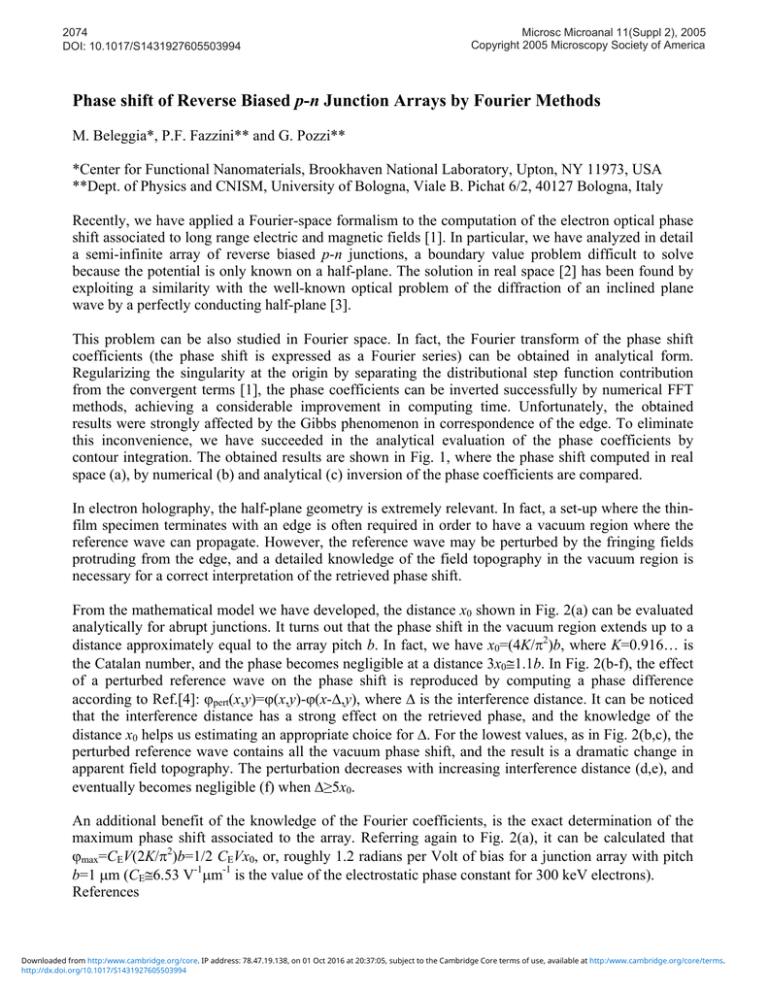
2074 DOI: 10.1017/S1431927605503994 Microsc Microanal 11(Suppl 2), 2005 Copyright 2005 Microscopy Society of America Phase shift of Reverse Biased p-n Junction Arrays by Fourier Methods M. Beleggia*, P.F. Fazzini** and G. Pozzi** *Center for Functional Nanomaterials, Brookhaven National Laboratory, Upton, NY 11973, USA **Dept. of Physics and CNISM, University of Bologna, Viale B. Pichat 6/2, 40127 Bologna, Italy Recently, we have applied a Fourier-space formalism to the computation of the electron optical phase shift associated to long range electric and magnetic fields [1]. In particular, we have analyzed in detail a semi-infinite array of reverse biased p-n junctions, a boundary value problem difficult to solve because the potential is only known on a half-plane. The solution in real space [2] has been found by exploiting a similarity with the well-known optical problem of the diffraction of an inclined plane wave by a perfectly conducting half-plane [3]. This problem can be also studied in Fourier space. In fact, the Fourier transform of the phase shift coefficients (the phase shift is expressed as a Fourier series) can be obtained in analytical form. Regularizing the singularity at the origin by separating the distributional step function contribution from the convergent terms [1], the phase coefficients can be inverted successfully by numerical FFT methods, achieving a considerable improvement in computing time. Unfortunately, the obtained results were strongly affected by the Gibbs phenomenon in correspondence of the edge. To eliminate this inconvenience, we have succeeded in the analytical evaluation of the phase coefficients by contour integration. The obtained results are shown in Fig. 1, where the phase shift computed in real space (a), by numerical (b) and analytical (c) inversion of the phase coefficients are compared. In electron holography, the half-plane geometry is extremely relevant. In fact, a set-up where the thinfilm specimen terminates with an edge is often required in order to have a vacuum region where the reference wave can propagate. However, the reference wave may be perturbed by the fringing fields protruding from the edge, and a detailed knowledge of the field topography in the vacuum region is necessary for a correct interpretation of the retrieved phase shift. From the mathematical model we have developed, the distance x0 shown in Fig. 2(a) can be evaluated analytically for abrupt junctions. It turns out that the phase shift in the vacuum region extends up to a distance approximately equal to the array pitch b. In fact, we have x0=(4K/π2)b, where K=0.916… is the Catalan number, and the phase becomes negligible at a distance 3x0≅1.1b. In Fig. 2(b-f), the effect of a perturbed reference wave on the phase shift is reproduced by computing a phase difference according to Ref.[4]: ϕpert(x,y)=ϕ(x,y)-ϕ(x-∆,y), where ∆ is the interference distance. It can be noticed that the interference distance has a strong effect on the retrieved phase, and the knowledge of the distance x0 helps us estimating an appropriate choice for ∆. For the lowest values, as in Fig. 2(b,c), the perturbed reference wave contains all the vacuum phase shift, and the result is a dramatic change in apparent field topography. The perturbation decreases with increasing interference distance (d,e), and eventually becomes negligible (f) when ∆≥5x0. An additional benefit of the knowledge of the Fourier coefficients, is the exact determination of the maximum phase shift associated to the array. Referring again to Fig. 2(a), it can be calculated that ϕmax=CEV(2K/π2)b=1/2 CEVx0, or, roughly 1.2 radians per Volt of bias for a junction array with pitch b=1 µm (CE≅6.53 V-1µm-1 is the value of the electrostatic phase constant for 300 keV electrons). References Downloaded from http:/www.cambridge.org/core. IP address: 78.47.19.138, on 01 Oct 2016 at 20:37:05, subject to the Cambridge Core terms of use, available at http:/www.cambridge.org/core/terms. http://dx.doi.org/10.1017/S1431927605503994 Microsc Microanal 11(Suppl 2), 2005 2075 [1] M. Beleggia et al., Ultramicroscopy 96 (2003) 93. [2] M. Beleggia et al., Philos. Mag. B 80 (2000) 1071. [3] F. Gori, Opt. Commun. 48 (1983) 67. [4] G. Matteucci et al., Advanc. Imag. Electron. Phys. 99 (1997) 171. [5] This work was supported by the U.S. Department of Energy, Basic Energy Sciences, contract number DE-AC02-98CH10886 and by MIUR, FIRB funding RBAU01M97L. FIG. 1. Comparison between the three different approaches for the computation of the p-n junction array phase shift (displayed as a 2× amplified cosine map): (a) real space approach, (b) numerical inversion and (c) analytical inversion of the phase coefficients (the series was truncated after six terms. The junctions are tilted at 35° with respect to the edge perpendicular. The computing times on a standard windows-PC with a 1 Ghz processor were, respectively, 550 s, 80 s, 15 s. FIG. 2. On the left: p-n junction phase shift profile across the edge, taken at the center of the p-region. On the right: effect of the perturbed reference wave on the reconstructed phase shift (displayed as a 10× amplified cosine map) of a p-n junction. The image size is 1×2 µm, and the interference distances are indicated in the images. Downloaded from http:/www.cambridge.org/core. IP address: 78.47.19.138, on 01 Oct 2016 at 20:37:05, subject to the Cambridge Core terms of use, available at http:/www.cambridge.org/core/terms. http://dx.doi.org/10.1017/S1431927605503994
