OP284A
Dual Operational Amplifier
VCC
RB1
OP284A
R3
R4
QB6
QB5
RB3
Q11
Q7
TP
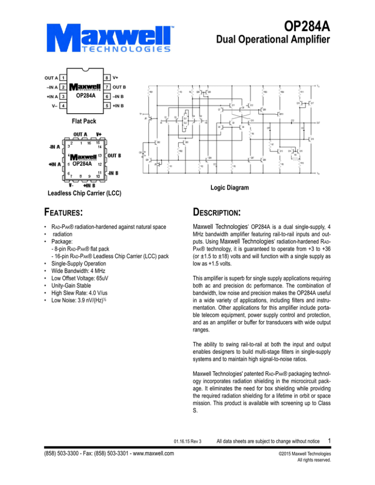
Flat Pack
Q1
JB1
Q3
QL1
-IN
Q4
Q8
RB4
Q16
Q12
Q17
QB9
QB10
Q2
QL2
R11
+IN
Q10
Q9
Q5
CC2
Q6
OUT
CFF
CO
R6
Q18
QB2
QB3
RB2
CB1 N+
M P+
OP284A
R7
Q13
Q14
Q15
R9
QB4
QB1
JB2
R1
R2
QB7
CC1
R5
QB8
R8
R10
VEE
Logic Diagram
FEATURES:
DESCRIPTION:
• RAD-PAK® radiation-hardened against natural space
• radiation
• Package:
- 8-pin RAD-PAK® flat pack
- 16-pin RAD-PAK® Leadless Chip Carrier (LCC) pack
• Single-Supply Operation
• Wide Bandwidth: 4 MHz
• Low Offset Voltage: 65uV
• Unity-Gain Stable
• High Slew Rate: 4.0 V/us
• Low Noise: 3.9 nV/(Hz)½
Maxwell Technologies’ OP284A is a dual single-supply, 4
MHz bandwidth amplifier featuring rail-to-rail inputs and outputs. Using Maxwell Technologies’ radiation-hardened RADPAK® technology, it is guaranteed to operate from +3 to +36
(or ±1.5 to ±18) volts and will function with a single supply as
low as +1.5 volts.
This amplifier is superb for single supply applications requiring
both ac and precision dc performance. The combination of
bandwidth, low noise and precision makes the OP284A useful
in a wide variety of applications, including filters and instrumentation. Other applications for this amplifier include portable telecom equipment, power supply control and protection,
and as an amplifier or buffer for transducers with wide output
ranges.
The ability to swing rail-to-rail at both the input and output
enables designers to build multi-stage filters in single-supply
systems and to maintain high signal-to-noise ratios.
Maxwell Technologies' patented RAD-PAK® packaging technology incorporates radiation shielding in the microcircuit package. It eliminates the need for box shielding while providing
the required radiation shielding for a lifetime in orbit or space
mission. This product is available with screening up to Class
S.
01.16.15 Rev 3
(858) 503-3300 - Fax: (858) 503-3301 - www.maxwell.com
All data sheets are subject to change without notice
1
©2015 Maxwell Technologies
All rights reserved.
Memory
Leadless Chip Carrier (LCC)
OP284A
Dual Operational Amplifier
TABLE 1. FLAT PACK PINOUT DESCRIPTION
PIN
SYMBOL
DESCRIPTION
1, 7
OUT A, B
2, 6
-IN A, B
Negative Inputs
3, 5
+IN A, B
Positive Inputs
4
V-
Ground
8
V+
Supply Voltage
Outputs
TABLE 2. LEADLESS CHIP CARRIER (LCC) PINOUT DESCRIPTION
PIN
SYMBOL
DESCRIPTION
1, 13
OUT A, B
3, 11
-IN A, B
Negative Inputs
5, 9
+IN A, B
Positive Inputs
7
V-
Ground
15
V+
Supply Voltage
Outputs
Memory
TABLE 3. OP284A ABSOLUTE MAXIMUM RATINGS
PARAMETER
Supply Voltage
Input Voltage
Differential Input
Voltage1
SYMBOL
MIN
MAX
UNIT
VCC
--
±18
V
VI
--
±18
V
VDIF
--
±0.6
V
Output Short-Circuit Duration to GND
Indefinite
Storage Temperature
TS
-65
+150
°C
Operating Temperature
TA
-40
+125
°C
Junction Temperature
TJ
-65
+150
°C
--
0.75
Grams
--
6.48
°C/W
Package Weight
JC
Thermal Impedance
1. For input voltages greater than 0.6 volts, the input current should be limited to less 5 mA to prevent degradation or destruction of
the input devices.
TABLE 4. DELTA LIMITS
PARAMETER
VARIATION
ICC
±10% of specified value in Table 5
01.16.15 Rev3
All data sheets are subject to change without notice
2
©2015 Maxwell Technologies
All rights reserved.
OP284A
Dual Operational Amplifier
TABLE 5. OP284A ELECTRICAL CHARACTERISTICS
(V+ = 15V, V- = -15V, VOUT = 0V, RS = 50, RL = 100K, VCM = 0V, TA = -40°C TO +125°C UNLESS OTHERWISE SPECIFIED.)
PARAMETER
Input offset voltage
SYMBOL
VIO
TEST CONDITIONS
+25°C
-40 to +125°C
Average offset voltage drift1
Offset voltage match1
VIOTC RL=2k
VIO |VIO (max) - VIO (min)|, +25°C
|VIO (max) - VIO (min)|, -40 to +125°C
Input bias current
IB
RS = 50, +25°C
RS = 50-40 to +125°C
Input offset current
IOS
RS =50, +25°C
RS = 50, -40 to +125°C
IIBTC
Input voltage range
IVR
Common mode rejection
ratio
Output current
RS = 50
+ICC
UNIT
1
-100
--
100
µV
2, 3
-200
--
205
1, 2, 3
--
--
2
µV/°C
1
-
--
100
µV
2, 3
-
--
200
1
-350
--
350
nA
2, 3
-575
--
575
nA
1
-35
--
35
nA
2, 3
-50
--
50
nA
--
200
pA/°C
-15
--
15
V
4,5,6
86
--
--
dB
VCM = -15V to +15V, TA=25°C
4
80
--
--
dB
VOUT = -10V, 1ms pulse, TA=25°C
1
10
--
--
mA
2, 3
5
--
--
1
--
-10
2, 3
--
-5
VOUT = +10V, 1ms pulse, TA=25°C
VOUT = -10V, 1ms pulse
Quiescent power supply
current per amplifier
MAX
1, 2, 3
VOUT = -10V, 1ms pulse
-IO
TYP
1, 2, 3
CMRR VCM = -14V to +14V
+IO
MIN
IOUT = 0mA VS=±18V, TA=25°C
mA
1
--
--
1.80
2, 3
--
--
2.25
1
-1.80
--
--
2, 3
2.25
--
--
Power supply rejection ratio +PSRR VS=±2V to ±18V
1, 2, 3
90
--
--
dB
-PSRR VS=±2V to ±18V
1, 2, 3
90
--
--
dB
0.1Hz to 10Hz, RL=2k,
CL=50pF, TA=+25°C
1
--
0.30
--
µVp-p
IOUT = 0mA VS=±18V
-ICC
IOUT = 0mA VS=±18V, TA=25°C
IOUT = 0mA VS=±18V
Low frequency, peak-topeak noise1
Enp-p
mA
mA
Input noise voltage density1
En
RS=20, fO=1kHz, RL=2k,
CL=50pF, TA=+25°C
1
--
3.9
--
nV/
(Hz)½
Input noise current density1
In
RS=20M, fO=1kHz, RL=2k,
CL=50pF, TA=+25°C
1
--
0.4
--
pA/
(Hz)½
Power consumption1,2
PC
+10V, IOUT=0mA, RL=2k
1, 2, 3
--
81
mW
Large signal voltage gain
AVO
+10V, RL=2.0k, TA=25°C
4
150
+10V, RL=2.0kTA=125°C
5,6
75
+VOUT1 IL=1.0mA
4,5,6
14.8
--
--
V
-VOUT1 IL=1.0mA
4,5,6
--
--
-14.8
V
4
--
4.25
--
MHz
Output voltage swing
Gain bandwidth product1
GBWP VO=200mV, RL=2.0k,
CL=50pF, TA=+25°C
01.16.15 Rev3
240
Memory
Input bias current drift1
SUBGROUPS
V/mV
All data sheets are subject to change without notice
3
©2015 Maxwell Technologies
All rights reserved.
OP284A
Dual Operational Amplifier
TABLE 5. OP284A ELECTRICAL CHARACTERISTICS
(V+ = 15V, V- = -15V, VOUT = 0V, RS = 50, RL = 100K, VCM = 0V, TA = -40°C TO +125°C UNLESS OTHERWISE SPECIFIED.)
PARAMETER
Full power bandwidth1,3
SYMBOL
TEST CONDITIONS
FPBW VPEAK=29vp-p, RL=2.0k,
CL=50pF, TA=+25°C, 1% distortion
SUBGROUPS
MIN
TYP
MAX
UNIT
4
--
35
--
kHz
Settling time
tS
AV=+1.0, CL=50pF, RL=2.0k
To 0.01%, 10V step
9
--
--
5
µs
Phase margin
FO
AV=1.0, CL=50pF,
RL=2.0k, TA=+25°C
4
--
--
50
Degrees
+SR
CL=50pF, RL=2.0k
4,5,6
2.4
4.0
--
V/µs
-SR
CL=50pF, RL=2.0k
4,5,6
2.4
4.0
--
V/µs
Slew rate
1. Guaranteed by design.
2. Power consumption is based upon quiescent supply current maximum test limit. No load on outputs.
3. Full power bandwidth is based on slew rate measurement using FBBW = slew rate/(2PVPEAK).
Memory
01.16.15 Rev3
All data sheets are subject to change without notice
4
©2015 Maxwell Technologies
All rights reserved.
OP284A
Dual Operational Amplifier
FIGURE 4. INPUT OFFSET VOLTAGE DRIFT DISTRIBUTION
FIGURE 2. INPUT OFFSET VOLTAGE DISTRIBUTION
FIGURE 5. INPUT OFFSET VOLTAGE DRIFT DISTRIBUTION
FIGURE 3. INPUT OFFSET VOLTAGE DISTRIBUTION
FIGURE 6. BIAS CURRENT VS. TEMPERATURE
Memory
FIGURE 1. INPUT OFFSET VOLTAGE DISTRIBUTION
01.16.15 Rev3
All data sheets are subject to change without notice
5
©2015 Maxwell Technologies
All rights reserved.
OP284A
Dual Operational Amplifier
FIGURE 7. INPUT BIAS CURRENT VS. COMMON-MODE
VOLTAGE
FIGURE 9. SUPPLY CURRENT VS. TEMPERATURE
FIGURE 10. SUPPLY CURRENT VS. SUPPLY VOLTAGE
Memory
FIGURE 8. OUTPUT VOLTAGE TO SUPPLY RAIL VS. LOAD
CURRENT
FIGURE 11. SHORT CIRCUIT CURRENT VS. TEMPERATURE
01.16.15 Rev3
All data sheets are subject to change without notice
6
©2015 Maxwell Technologies
All rights reserved.
OP284A
Dual Operational Amplifier
FIGURE 12. OPEN-LOOP GAIN AND PHASE VS. FREQUENCY
(NO LOAD)
FIGURE 14. OPEN-LOOP GAIN AND PHASE VS. FREQUENCY
(NO LOAD)
FIGURE 13. OPEN-LOOP GAIN AND PHASE VS. FREQUENCY
(NO LOAD)
FIGURE 15. OPEN-LOOP GAIN VS. TEMPERATURE
Memory
01.16.15 Rev3
All data sheets are subject to change without notice
7
©2015 Maxwell Technologies
All rights reserved.
OP284A
Dual Operational Amplifier
FIGURE 16. CLOSED-LOOP GAIN VS. FREQUENCY (2KW
LOAD)
FIGURE 18. CLOSED-LOOP GAIN VS. FREQUENCY (2KW
LOAD)
FIGURE 19. OUTPUT IMPEDANCE VS. FREQUENCY
01.16.15 Rev3
Memory
FIGURE 17. CLOSED-LOOP GAIN VS. FREQUENCY (2KW
LOAD)
All data sheets are subject to change without notice
8
©2015 Maxwell Technologies
All rights reserved.
OP284A
Dual Operational Amplifier
FIGURE 20. OUTPUT IMPEDANCE VS. FREQUENCY
FIGURE 23. MAXIMUM OUTPUT SWING VS. FREQUENCY
FIGURE 21. OUTPUT IMPEDANCE VS. FREQUENCY
FIGURE 24. CMMR VS. FREQUENCY
Memory
FIGURE 22. MAXIMUM OUTPUT SWING VS. FREQUENCY
01.16.15 Rev3
All data sheets are subject to change without notice
9
©2015 Maxwell Technologies
All rights reserved.
OP284A
Dual Operational Amplifier
FIGURE 25. PSRR VS. FREQUENCY
FIGURE 27. SLEW RATE VS. TEMPERATURE
FIGURE 28. VOLTAGE NOISE DENSITY VS. FREQUENCY
Memory
FIGURE 26. SMALL SIGNAL OVERSHOOT VS. CAPACITIVE
LOAD
FIGURE 29. CURRENT NOISE DENSITY VS. FREQUENCY
01.16.15 Rev3
All data sheets are subject to change without notice
10
©2015 Maxwell Technologies
All rights reserved.
OP284A
Dual Operational Amplifier
FIGURE 30. SETTLING TIME VS. STEP SIZE
FIGURE 33. 0.1 HZ TO 10 HZ NOISE
FIGURE 31. SETTLING VS. STEP SIZE
FIGURE 34. CHANNEL SEPARATION VS. FREQUENCY
Memory
FIGURE 32. 0.1 HZ TO 10 HZ NOISE
01.16.15 Rev3
All data sheets are subject to change without notice
11
©2015 Maxwell Technologies
All rights reserved.
OP284A
Dual Operational Amplifier
FIGURE 35. SMALL SIGNAL TRANSIENT RESPONSE
FIGURE 38. SMALL SIGNAL TRANSIENT RESPONSE
FIGURE 39. TOTAL HARMONIC DISTORTION VS. FREQUENCY
FIGURE 36. SMALL SIGNAL TRANSIENT RESPONSE
Memory
FIGURE 37. SMALL SIGNAL TRANSIENT RESPONSE
01.16.15 Rev3
All data sheets are subject to change without notice
12
©2015 Maxwell Technologies
All rights reserved.
OP284A
Dual Operational Amplifier
Memory
8-PIN RAD-PAK® FLAT PACKAGE
SYMBOL
DIMENSION
MIN
NOM
MAX
A
0.119
0.132
0.149
b
0.010
0.017
0.022
c
0.004
0.005
0.009
D
0.250
0.255
0.260
E
0.250
0.255
0.260
E1
--
--
0.290
E2
0.125
0.145
--
E3
0.030
0.040
--
e
0.050 BSC
L
0.338
0.348
0.358
Q
0.021
0.025
0.045
S1
0.005
0.019
--
N
8
Note: All dimensions in inches
01.16.15 Rev3
All data sheets are subject to change without notice
13
©2015 Maxwell Technologies
All rights reserved.
OP284A
Dual Operational Amplifier
16-PIN RAD-PAK® LCC PACKAGE
SYMBOL
DIMENSION
NOM
MAX
A
0.123
0.135
0.150
b
0.018
0.020
0.025
D
0.245
0.250
0.260
D1
0.150 BSC
S1
0.050 BSC
e
0.050 BSC
A1
0.095
0.105
N
Memory
MIN
0.116
16
Note: All dimensions in inches.
01.16.15 Rev3
All data sheets are subject to change without notice
14
©2015 Maxwell Technologies
All rights reserved.
OP284A
Dual Operational Amplifier
Important Notice:
These data sheets are created using the chip manufacturer’s published specifications. Maxwell Technologies verifies
functionality by testing key parameters either by 100% testing, sample testing or characterization.
The specifications presented within these data sheets represent the latest and most accurate information available to
date. However, these specifications are subject to change without notice and Maxwell Technologies assumes no
responsibility for the use of this information.
Maxwell Technologies’ products are not authorized for use as critical components in life support devices or systems
without express written approval from Maxwell Technologies.
Any claim against Maxwell Technologies must be made within 90 days from the date of shipment from Maxwell Technologies. Maxwell Technologies’ liability shall be limited to replacement of defective parts.
Memory
01.16.15 Rev3
All data sheets are subject to change without notice
15
©2015 Maxwell Technologies
All rights reserved.
OP284A
Dual Operational Amplifier
Product Ordering Options
Model Number
OP284A
RP
F
X
Option Details
Feature
Monolithic
S = Maxwell Class S
B = Maxwell Class B
I = Industrial (testing @ -40°C,
+25°C, +125°C)
E = Engineering (testing @ +25°C)
Package
F = Flat Pack
L = Leadless Chip Carrier (LLC)
Radiation Feature
RP = RAD-PAK® package
Base Product
Nomenclature
Operational Amplifier
01.16.15 Rev3
All data sheets are subject to change without notice
16
©2015 Maxwell Technologies
All rights reserved.
Memory
Screening Flow


