University of Wyoming EE 2390 Digital Systems Design Spring
advertisement

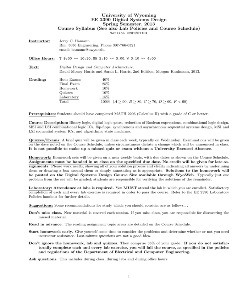
University of Wyoming EE 2390 Digital Systems Design Spring Semester, 2013 Course Syllabus (See also Lab Policies and Course Schedule) Version <20130110> Instructor: Jerry C. Hamann Rm. 5036 Engineering, Phone 307-766-6321 email: hamann@uwyo.edu Office Hours: T 9:00 -- 10:30, MW 2:10 -- 3:00, W 3:10 -- 4:00 Text: Digital Design and Computer Architecture, David Money Harris and Sarah L. Harris, 2nd Edition, Morgan Kaufmann, 2013. Grading: Hour Exams Final Exam Homework Quizzes Laboratory Total 40% 25% 10% 10% 15% 100% (A ≥ 90, B ≥ 80, C ≥ 70, D ≥ 60, F < 60) Prerequisites: Students should have completed MATH 2205 (Calculus II) with a grade of C or better. Course Description: Binary logic, digital logic gates, reduction of Boolean expressions, combinational logic design. MSI and LSI combinational logic ICs, flip-flops, synchronous and asynchronous sequential systems design, MSI and LSI sequential system ICs, and algorithmic state machines. Quizzes/Exams: A brief quiz will be given in class each week, typically on Wednesday. Examinations will be given on the days noted on the Course Schedule, unless circumstances dictate a change which will be announced in class. It is not possible to make up a missed quiz or exam without a University Excused Absence. Homework: Homework sets will be given on a near weekly basis, with due dates as shown on the Course Schedule. Assignments must be handed in at class on the specified due date. No credit will be given for late assignments. Please work neatly, showing all of your solution process and clearly indicating all answers by underlining them or drawing a box around them or simply annotating as is appropriate. Solutions to the homework will be posted on the Digital Systems Design Course Site available through WyoWeb. Typically just one problem from the set will be graded; students are responsible for verifying the solutions of the remainder. Laboratory: Attendance at labs is required. You MUST attend the lab in which you are enrolled. Satisfactory completion of each and every lab exercise is required in order to pass the course. Refer to the EE 2390 Laboratory Policies handout for further details. Suggestions: Some recommendations for study which you should consider are as follows. . . Don’t miss class. New material is covered each session. If you miss class, you are responsible for discovering the missed material. Read in advance. The reading assignment topic areas are detailed on the Course Schedule. Start homework early. Give yourself some time to consider the problems and determine whether or not you need instructor assistance. Last-minute questions are not a good idea. Don’t ignore the homework, lab and quizzes. They comprise 35% of your grade. If you do not satisfactorally complete each and every lab exercise, you will fail the course, as specified in the policies and regulations of the Department of Electrical and Computer Engineering. Ask questions. This includes during class, during labs and during office hours. 1 Objectives: At the end of the semester, students will be able to: • Manipulate fixed-width binary number representations in signed and unsigned formats to provide computations including addition and subtraction, with representations of such data in binary, octal, decimal and hexadecimal bases. • Apply analysis skills to correctly describe the behavior of combinational and synchronous sequential digital circuits. • Apply design skills to implement and test combinational and synchronous sequential digital circuits in both simulation (using a hardware descriptive language) and hardware prototype (using SSI, MSI, CPLD and FPGA) forms. • Demonstrate hands-on skills with use of contemporary digital electronic design software, the application of benchtop prototyping equipment, and the documentation of engineering design processes via a professional lab notebook. Engineering Notebook Policies: To encourage student development of a personal, professional engineering notebook, the quizzes and exams will be closed-book and closed-note with the exception of one reference: the student’s personal, bound engineering notebook, hereafter referred to as the “Lab Notebook.” Specifications for an allowable Lab Notebook are as follows: • Notebook format is permanent binding with no removable pages, page dimensions not to exceed A4 in area. • Outside cover and front inside cover page should clearly identify (1) student owner by name and contact info, (2) course by number and title, and (3) initial date of entries. • Each internal page should be individually and consecutively numbered, beginning with a table of contents on pages 1 thru 4. Pages should be filled successively, dated and signed. • All entries must be made in indelible ink or be permanently afixed to each individual page (in the case of computer printouts or similar materials) by careful cutting and sizing then afixing fully, on all edges, with transparent tape (absolutely no staples allowed). Corrections should be made with simple line-outs then signed and dated. Notebooks which include any looseleaf (unattached) materials or non-indelible (e.g. pencil) entries may not be used on any quiz or exam (the use of such a notebook will be considered a breach of academic/professional honesty and decorum, resulting in zero credit). Policies Regarding Assignments / Collaboration / Academic Dishonesty: Students are encouraged to discuss course topics and assignments with one another. However, the homework solutions, prelabs, quizzes and exams turned in by each student must consist of that individual’s own work as noted in the Department of Electrical and Computer Engineering Course Policies (available in the Department Office) and the University of Wyoming Academic Policies and Procedures. Failure to observe these expectations will result in sanctions as prescribed in University Regulation 6-802. Possible penalties include a grade of F for the course. Disability Services: Students with a physical, learning or psychological disability requiring accommodations must register with and provide documentation to the University Disability Support Services (UDSS) in the Student Educational Opportunity Office, Knight Hall room 330. Please contact your course instructor as soon as possible to complete plans for providing accommodations. 2 University of Wyoming Hamann EE 2390 ---Digital Systems Design Course Schedule of Lectures, Homework Assignments, and Exams Subject to Change, Check Version Date Version <20130110> Week 1 2 3 4 5 6 7 8 9 Spring Break 10 11 12 13 14 15 Lecture Number Date 1 14-Jan-2013 M Intro to Digital Systems, Binary Number Systems, Hex and Octal Ch. 1, pp. 3--14 2 16-Jan-2013 W Number Complements, Arithmetic Addition and Subtraction Ch. 1, pp. 14--19 Binary Codes, BCD, Excess-3, Gray Code, ASCII, Parity Notes Day of Week Text Reading Topic 3 18-Jan-2013 F No Class 21-Jan-2013 M 4 23-Jan-2013 W Logic Gates and Physical Implementations Ch. 1, pp. 19--26 5 25-Jan-2013 F Combinational Logic Terminology Ch. 2, pp. 55--60 6 28-Jan-2013 M Boolean Algebra Axioms and Theorems Ch. 2, pp. 60--66 7 30-Jan-2013 W Digital Logic Gates, Schematics, Manipulations Ch. 2, pp. 66--75 8 1-Feb-2013 F Gate-Level Minimization, Karnaugh Maps Ch. 2, pp. 75--81 Ch. 2, pp. 81--83 1/1 HWK Due Wyoming Equality Day -- Classes Excused 9 4-Feb-2013 M More Karnaugh Maps, Don't Cares, NAND-NAND / NOR-NOR 10 6-Feb-2013 W Introduction to HDLs Ch. 4, pp. 173--186 11 8-Feb-2013 F Combinational Logic Building Blocks Ch. 2, pp. 83--88 12 11-Feb-2013 M Timing and Glitches Ch. 2, pp. 88--95 13 13-Feb-2013 W More Verilog HDL for Combinational Logic Ch. 4, pp. 186--193 14 15-Feb-2013 F More HDL, Test Benches Ch. 4, pp. 220--224 15 18-Feb-2013 M Intro Synchronous Sequential Logic Systems Ch. 3, pp. 109--113 16 20-Feb-2013 W Flip-Flop Storage Elements Ch. 3, pp. 114-118 17 22-Feb-2013 F Synchronous Logic Design Ch. 3, pp. 119--123 18 25-Feb-2013 M Summary for Exam #1 19 27-Feb-2013 W 20 1-Mar-2013 F Design and Analysis of Synchronous State Machines Ch. 3, pp. 123--141 21 4-Mar-2013 M Sequential Logic Description with Verilog HDL Ch. 4, pp. 193--209 22 6-Mar-2013 W More Finite State Machine Synthesis with Verilog HDL Ch. 4, pp. 209--213 23 8-Mar-2013 F State Reduction and Assignment, Excitation Tables Notes 24 11-Mar-2013 M More State Machine Design Notes 25 13-Mar-2013 W Counters and Examples Ch. 5, pp. 260--261 26 15-Mar-2013 F Registers and Examples Ch. 5, pp. 261--263 Set #1 Due Set #2 Due Set #3 Due Set #4 Due Set #5 Due Exam #1 No Class 18-Mar-2013 M Spring Break No Class 20-Mar-2013 W No Classes No Class 22-Mar-2013 F 27 25-Mar-2013 M Verilog HDL for Registers and Counters Notes 28 27-Mar-2013 W Introduction to Register Transfer Level Notation Notes No Class 29-Mar-2013 F 29 1-Apr-2013 M ASM Design Example Notes 30 3-Apr-2013 W ASM Description in Verilog HDL Notes 31 5-Apr-2013 F Complex ASM Design in Verilog HDL Notes 32 8-Apr-2013 M Summary for Exam #2 33 10-Apr-2013 W 34 12-Apr-2013 F Advanced ASM Design Techniques Notes 35 15-Apr-2013 M Advanced Arithmetic Circuits Ch. 5, pp. 239--254 36 17-Apr-2013 W Advanced Number Systems Ch. 5, pp. 255--259 37 19-Apr-2013 F Memory, Ram Operations and Verilog HDL Description Ch. 5, pp. 263--272 38 22-Apr-2013 M PLAs, PLDs, CPLDs and FPGAs Ch. 5, pp. 272--280 39 24-Apr-2013 W Error Detection and Correction Examples Notes 40 26-Apr-2013 F Advanced Digital Design Notes 41 29-Apr-2013 M Advanced Digital Design Notes 42 1-May-2013 W Advanced Digital Design Notes 43 3-May-2013 F Summary for Exam #3 Final Exam 10-May-2013 F Set #6 Due Set #7 Due No Labs Set #8 Due Good Friday -- Classes Excused Set #9 Due Exam #2 Final Exam (8:00 am - 10:00 am) Set #10 Due Set #11 Due Set #12 Due


