Nanocomposite titanium dioxide/polymer photovoltaic cells: effects
advertisement
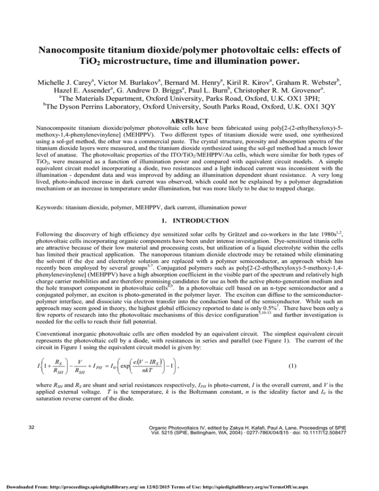
Nanocomposite titanium dioxide/polymer photovoltaic cells: effects of TiO2 microstructure, time and illumination power. Michelle J. Careya, Victor M. Burlakova, Bernard M. Henrya, Kiril R. Kirova, Graham R. Websterb, Hazel E. Assendera, G. Andrew D. Briggsa, Paul L. Burnb, Christopher R. M. Grovenora. a The Materials Department, Oxford University, Parks Road, Oxford, U.K. OX1 3PH; b The Dyson Perrins Laboratory, Oxford University, South Parks Road, Oxford, U.K. OX1 3QY ABSTRACT Nanocomposite titanium dioxide/polymer photovoltaic cells have been fabricated using poly[2-(2-ethylhexyloxy)-5methoxy-1,4-phenylenevinylene] (MEHPPV). Two different types of titanium dioxide were used, one synthesized using a sol-gel method, the other was a commercial paste. The crystal structure, porosity and absorption spectra of the titanium dioxide layers were measured, and the titanium dioxide synthesized using the sol-gel method had a much lower level of anatase. The photovoltaic properties of the ITO/TiO2/MEHPPV/Au cells, which were similar for both types of TiO2, were measured as a function of illumination power and compared with equivalent circuit models. A simple equivalent circuit model incorporating a diode, two resistances and a light induced current was inconsistent with the illumination - dependent data and was improved by adding an illumination dependent shunt resistance. A very long lived, photo-induced increase in dark current was observed, which could not be explained by a polymer degradation mechanism or an increase in temperature under illumination, but was more likely to be due to trapped charge. Keywords: titanium dioxide, polymer, MEHPPV, dark current, illumination power 1. INTRODUCTION Following the discovery of high efficiency dye sensitized solar cells by Grätzel and co-workers in the late 1980s1,2, photovoltaic cells incorporating organic components have been under intense investigation. Dye-sensitized titania cells are attractive because of their low material and processing costs, but utilization of a liquid electrolyte within the cells has limited their practical application. The nanoporous titanium dioxide electrode may be retained while eliminating the solvent if the dye and electrolyte solution are replaced with a polymer semiconductor, an approach which has recently been employed by several groups3-7. Conjugated polymers such as poly[2-(2-ethylhexyloxy)-5-methoxy-1,4phenylenevinylene] (MEHPPV) have a high absorption coefficient in the visible part of the spectrum and relatively high charge carrier mobilities and are therefore promising candidates for use as both the active photo-generation medium and the hole transport component in photovoltaic cells8,9. In a photovoltaic cell based on an n-type semiconductor and a conjugated polymer, an exciton is photo-generated in the polymer layer. The exciton can diffuse to the semiconductorpolymer interface, and dissociate via electron transfer into the conduction band of the semiconductor. While such an approach may seem good in theory, the highest global efficiency reported to date is only 0.5%7. There have been only a few reports of research into the photovoltaic mechanisms of this device configuration5,10-13 and further investigation is needed for the cells to reach their full potential. Conventional inorganic photovoltaic cells are often modeled by an equivalent circuit. The simplest equivalent circuit represents the photovoltaic cell by a diode, with resistances in series and parallel (see Figure 1). The current of the circuit in Figure 1 using the equivalent circuit model is given by: I .1 + RS V e.(V − IR S ) − + I PH = I 0 . exp − 1 , R SH RSH nkT (1) where RSH and RS are shunt and serial resistances respectively, IPH is photo-current, I is the overall current, and V is the applied external voltage. T is the temperature, k is the Boltzmann constant, n is the ideality factor and I0 is the saturation reverse current of the diode. 32 Organic Photovoltaics IV, edited by Zakya H. Kafafi, Paul A. Lane, Proceedings of SPIE Vol. 5215 (SPIE, Bellingham, WA, 2004) · 0277-786X/04/$15 · doi: 10.1117/12.508477 Downloaded From: http://proceedings.spiedigitallibrary.org/ on 12/02/2015 Terms of Use: http://spiedigitallibrary.org/ss/TermsOfUse.aspx Figure 1. A simple equivalent circuit model of a photovoltaic device. RSH and RS are shunt and serial resistances respectively, IPH is photo-current, I is the overall current, and V is the applied external voltage. Equivalent circuit models with a diode have also been used to evaluate the performance of organic/TiO2 interfaces14,15 as the diode equation is valid generally for interfacial electron transfer16. We have assumed that the electron transfer at the TiO2/polymer interface is the controlling factor in the device performance and have modeled the interface as a diode. This article reports preliminary results from an on-going investigation of photovoltaic cells based on nanocrystalline titanium dioxide and MEHPPV. Two different methods have been used to fabricate the TiO2 and these layers, together with MEHPPV have been extensively characterized using a range of analytical techniques including atomic force microscopy (AFM), X-ray diffraction (XRD) and U.V.-visible spectroscopy. The photovoltaic characteristics of cells incorporating these layers have been measured and compared with simple equivalent circuit models. 2. EXPERIMENTAL PROCEDURE Photovoltaic devices with an ITO/TiO2/MEHPPV/Au configuration were formed on pre-patterned ITO/glass. TiO2 dispersions created via two different processes were used to make the TiO2 layers. In a sol-gel process, TiO2 dispersions were synthesized according to a literature method17, but without the concentration and autoclaving steps. A surfactant, Triton-X-100, was added to the TiO2 dispersion and it was deposited onto pre-patterned ITO/glass by spincoating at 2000 r.p.m. for 120 seconds. The film was then annealed at 450 °C for 20 minutes before spin-coating again. Transparent thin films of 140 nm thickness were obtained by three sequential spin-coating and annealing steps. The synthesised sol-gel dispersion was compared with Ti-Nanoxide HT (Solaronix SA, Switzerland). The synthesis of Ti-Nanoxide HT incorporates a step inducing anatase formation. A doctor blade was used to apply layers of 1.8 µm thickness onto ITO/glass substrates. The deposited layers were allowed to dry at 100 °C for a few minutes before annealing in air at 450 °C for 10 hours in a furnace oven, conditions which created the greatest TiO2 surface area. MEHPPV was synthesized according to a well established procedure18. MEHPPV films, ranging from 40 to 120 nm thick, were spin-coated on top of the TiO2 layers from chlorobenzene solutions at a spin speed of 2000 rpm for 40 seconds. The devices were completed by evaporation of Au electrodes (45 nm thick) with the gold being deposited at a rate of 20 Å/min at a vacuum of ≈ 10-6 mbar. The active area of each device was 0.062 cm2. Characterisation of the TiO2 and MEHPPV was conducted using a range of analytical techniques. The thickness of the TiO2 and polymer layers was determined using AFM in the contact mode (CP model, Park Instruments). The surface morphology of the layers was investigated using both SEM and AFM. Optical absorption spectra of the films were measured using a Perkin Elmer Lambda 14P spectrometer. Gas adsorption was performed on a six-port Quantachrome AS6B-KR Autosorb gas sorption system using N2 gas. IV measurements of the ITO/TiO2/MEHPPV/Au devices were carried out both in the dark and under illumination using a Keithley 2400 source meter. The photo-current measurements were performed using a halogen light source with emission between 400 and 700 nm. The samples were mounted in an Oxford Instruments DN series cryostat and evacuated to about 2.5x10⁻² mbar prior to the measurements. For the dark current J-V measurements the sample was retained in the dark and under a vacuum of 2.5x10⁻² mbar overnight prior to illumination for 101 minutes through Tech SpecTM heat absorbing glass at 120 mW/cm2. For the purpose of these measurements a positive voltage on the gold electrode was assigned a positive bias. Proc. of SPIE Vol. 5215 Downloaded From: http://proceedings.spiedigitallibrary.org/ on 12/02/2015 Terms of Use: http://spiedigitallibrary.org/ss/TermsOfUse.aspx 33 3. RESULTS AND DISCUSSION 3.1 Microstructural Study of TiO2 3.1.1 Ti-Nanoxide HT (Anatase Paste) TiO2 layers formed from the commercial Ti-Nanoxide HT paste appeared transparent but absorbed light below about 370 nm, which is consistent with the anatase band gap of 3.2eV (about 385 nm). An XRD study of the layer detected only a crystalline phase of anatase. A typical diffraction pattern featuring anatase reflections is shown in Figure 2. The width of the XRD reflections is related to the size of the crystallites by the Scherrer equation, β= 0. 9λ , t cos θ (2) where β = the breadth of diffracted rays due to the crystallite size, λ = the X-ray wavelength, t = the crystallite size and θ = the Bragg angle of diffracted rays19. Based on the peak widths shown in Figure 2, the average dimension of the crystallites was found to be 18 nm. The surface morphology of the TiO2 layers deposited on ITO was examined using SEM and AFM. Figure 3 shows an SEM image of an annealed TiO2 layer. The layer is porous and consists of agglomerates of TiO2 crystallites of average size about 50 nm. The agglomerates have also been observed using AFM (see Figure 3) which indicated that the surface roughness is approximately 10 nm. (101) Intensity / counts 250 (004) 200 (200) (105) and (211) 150 100 50 0 20 25 30 35 40 45 50 55 60 Angle / 2θ Figure 2. XRD patterns of annealed films of TiO2 featuring diffraction by the crystal planes of anatase. The higher intensity data was produced by the Ti-Nanoxide HT paste while the lower intensity data was produced by the synthesized sol-gel dispersion. The peaks are labeled to the corresponding diffracting plane. Gas adsorption experiments were performed to establish the porosity of the TiO2 layers derived from the anatase paste, comparing 1 and 10 hour annealing times. The N2 adsorption isotherms of the TiO2 layers were found to correspond to type IV of the IUPAC classification indicating that the films are mesoporous, with a surface area of 175.3 m2g-1, pore volume of 0.42cm3g-1 and average pore diameter of 9 nm. The majority of pores are cylindrical in shape with a narrow size distribution. 34 Proc. of SPIE Vol. 5215 Downloaded From: http://proceedings.spiedigitallibrary.org/ on 12/02/2015 Terms of Use: http://spiedigitallibrary.org/ss/TermsOfUse.aspx Figure 3. SEM (left) and AFM (right) images of films TiO2 produced from the Ti-Nanoxide HT paste annealed for 10 hours at 450ºC. 3.1.2 Characterization of Synthesised Sol-Gel TiO2 X-ray diffraction and TEM studies established that films of the synthesised sol-gel titanium dioxide were predominately amorphous prior to annealing. Annealing of the deposited sol-gel layers in an air ambient had a strong influence on the structure of the films. For the photovoltaic cells a heat treatment of 450 °C was used. X-ray diffraction measurements confirmed the presence of anatase (see Figure 2), although the signal was too weak for reliable measurement of the crystallite size. The annealed films were highly transparent with the onset of UV absorption at about 340 nm in comparison to about 370 nm in the Ti-Nanoxide HT case. A comparison of the absorption spectra of the 0.14 µm solgel and 0.5 and 1.8 µm Ti-Nanoxide HT layers (see Figure 4) indicated that the thickness of the layers was insufficient to fully explain the onset of absorption, and the anatase level in the annealed sol-gel film was low. Absorbance AFM measurements indicated that the surface morphology of these layers consisted of particles of varying average size 100 – 400 nm and a roughness of about 2 nm (Figure 5). However, a high magnification AFM scan found evidence of smaller features 20-30 nm in size. 2 1.8 1.6 1.4 1.2 1 0.8 0.6 0.4 0.2 0 300 350 400 450 500 550 600 650 700 Wavelength / nm Figure 4. Absorption spectra of annealed 0.14 µm sol-gel TiO2 (dotted line), 1.8 µm Ti-Nanoxide HT paste (solid line) and 0.5 µm Ti-Nanoxide HT paste (dashed line). Proc. of SPIE Vol. 5215 Downloaded From: http://proceedings.spiedigitallibrary.org/ on 12/02/2015 Terms of Use: http://spiedigitallibrary.org/ss/TermsOfUse.aspx 35 Figure 5. AFM image of a sol-gel TiO2 sample annealed at 450°C. 3.2 PHOTOVOLTAIC CHARACTERISTICS 3.2.1 Open circuit voltage (VOC) and short circuit current density (JSC) Current density (J) of ITO/TiO2/MEHPPV/Au devices was measured as a function of applied bias (V) in the dark and under illumination. Devices made using the synthesised sol-gel and Ti-Nanoxide HT performed similarly, both producing global efficiencies of about 0.1 % and VOC around 1 V at 100 mWcm-2. The photovoltaic performance was consistent with similar measurements reported by other groups,5,10 but it is surprising that the high anatase, thicker and rougher Ti-Nanoxide HT layers did not produce efficiencies orders of magnitude higher than the partially crystalline sol-gel TiO2. The insensitivity to the combination of roughness and anatase content could be due to the use of the spincoating process, where the polymer presumably did not have time to enter the pores in the Ti-Nanoxide HT TiO2. Intensity dependent measurements on devices fabricated from the synthesized sol-gel titanium dioxide showed that the JSC was linearly dependent on light intensity, (see Figure 6) while the VOC had a logarithmic dependence, leveling off only at intensities close to 100 mWcm-2. A logarithmic relationship between VOC and illumination intensity is common at low current densities, for example in silicon and other crystalline cells20,21 and polymer blends22 and can be derived from the simple equivalent circuit model assuming the photocurrent is proportional to the illumination power and the shunt resistance is very high. Figure 6 contains a plot of VOC versus illumination power of an ITO/TiO2/MEHPPV/Au device with two theoretical curves derived from two different models. The dotted line is derived from the simple equivalent circuit model (Equation 1), while the solid line is derived by assuming that the shunt resistance is intensity dependent: R SH = max VOC J PH (3) max where VOC is the highest open circuit voltage achievable by the cell. The relationship between VOC and JPH then becomes: max VOC − VOC .1 − JO e.VOC exp − 1 = 0 J PH n.kT (4) An illumination intensity-dependent shunt resistance could be due to such phenomena as changes in recombination, charge carrier mobility or charge density under illumination. The equivalent circuit model incorporating the intensity dependent shunt resistance (Equation 4) models the VOC versus illumination power data much better than the simple equivalent circuit model (Equation 1) and provides plausible values for the leakage current density, J0 and the ideality factor, n. The requirement for an intensity dependent parameter implies that a photo-induced change occurs in ITO/TiO2/MEHPPV/Au cells. 36 Proc. of SPIE Vol. 5215 Downloaded From: http://proceedings.spiedigitallibrary.org/ on 12/02/2015 Terms of Use: http://spiedigitallibrary.org/ss/TermsOfUse.aspx 1.1 VOC / V 1.0 10-2 0.9 0.8 10-4 0.7 0.6 10-6 0.5 Current Density / mAcm-2 100 1.2 0.4 0.1 0 1 10 100 -2 Illumination Power / mWcm 1000 Figure 6. The effect of illumination power on the JSC and VOC of an ITO/TiO2/MEHPPV/Au cell prepared using the synthesized sol-gel TiO2. JSC data is accompanied by a linear fit. The circles are the VOC data and the solid line was obtained by numerical solution of the equivalent circuit model with intensity dependent shunt resistance, assuming the photocurrent was proportional to the illumination power. The parameters of the fit are J0 = 0.0006, n = 3.3 and max VOC = 1.05. The dotted line was obtained similarly from the simple equivalent circuit model. 3.2.2 Dark Current Current Density / A cm -2 The dark current under bias of the ITO/TiO2/MEHPPV/Au devices has been found to increase after illumination. It increased by as much as several orders of magnitude depending on the intensity and duration of the illumination. When measured under vacuum (2.5x10⁻² mbar) the photo-induced dark current reduced by an order of magnitude in about twenty minutes, but when given sufficient initial illumination, for example 101 minutes at 120 mW/cm2, only returned to its original level on the timescale of days (see Figure 7). The photovoltaic performance of the device shown in Figure 7 was measured after the dark current had decayed for 4 days. The VOC had risen from 0.7 V to 0.8 V, while the JSC and global efficiency had not changed. 10 -5 10 -6 10 -7 10 -8 (b) (c) (d) (a) 10 -9 10 -10 -0.4 0.0 0.4 0.8 1.2 Applied Bias /V Figure 7. Dark J-V curves of an ITO/TiO2(synthesized sol-gel)/MEHPPV/Au device (a) before, (b) 1 hour after illumination at about 120mWcm-2 for 101 minutes, (c) 1 day after illumination and (d) 4 days later. Proc. of SPIE Vol. 5215 Downloaded From: http://proceedings.spiedigitallibrary.org/ on 12/02/2015 Terms of Use: http://spiedigitallibrary.org/ss/TermsOfUse.aspx 37 The two equivalent circuit models used to analyse the PV response do not consider any time dependent processes and are therefore inadequate to describe these very long-lived transient phenomena. There could be a number of different reasons for an increase in dark current in the device, for example trapped charge in the nanoporous titanium dioxide layers16,23,24 or the MEHPPV, the presence of mobile ions, photo-oxidation of the polymer or an increase in temperature. Conductivity of MEHPPV can be enhanced by photo-oxidation,25,26 hence the observed increase in dark current could feasibly be due to polymer oxidation. However oxidation of the polymer is not reversible and is therefore inconsistent with eventual return to the original dark current density and subsequent measurement of the original photovoltaic efficiency. The mobility of charges in MEHPPV has also been reported to increase with increasing temperature.27 In our experiments, the device temperature is increased by the illumination and therefore the temperature dependence of the dark current was examined as a possible reason for the illumination-dependent dark current increase (see Figure 8a). The heating element in the cryostat was used to raise the temperature of the device to 30 °C then 50 °C and the dark current measured at a bias of 1 V. The heating element was then turned off and a further dark current measurement taken half an hour later, at about 40 °C. These measurements correspond to the filled circles in Figure 8a. Increasing the temperature by almost 30 °C increased the dark current by less than an order of magnitude. While the device was cooling, it was illuminated at 100 mW/cm2 for about 5 minutes. The light was switched off and the current at 1 V bias was then measured within 2 minutes. This first dark current measurement after illumination appears on both Figures 8a and 8b, at about 10-6 Acm-2, more than two orders of magnitude greater than before the illumination. For the next 15 minutes, both the dark current and the temperature were reducing and it appeared that the reduction in dark current could have been due to the reduction in temperature. To eliminate that possibility, the temperature was set to 50 °C, the temperature rose again, but the dark current continued to fall, indicating that an increase in temperature during illumination was not the sole cause of the increase in dark current. (a) (b) 1.E-05 1.E-05 after illumination 1.E-06 1.E-07 1.E-08 1.E-09 Current density / A cm-2 Current density / A cm -2 before illumination 1.E-06 1.E-07 1.E-08 20 30 40 50 Temperature / °C 60 10 100 1000 10000 Time After Illumination / s Figure 8. Dark current of an ITO/TiO2 (sol-gel)/MEHPPV/Au device at 1V bias, as a function of (a) temperature and (b) time after illumination. A mechanism involving mobile oxygen radical anions has been proposed to explain an increase in dark conductivity after irradiation of TiO2 / phthalocyanine solar cells in air.28 To test the possibility that the dark current observations reported here were due to the same mechanism, a high dark current was induced in an ITO/TiO2 (Ti-Nanoxide HT)/MEHPPV/Au device under vacuum, and air allowed into the sample chamber to observe the dark current decay. The dark current reduced to its initial level in less than 2 seconds, the resolution of the measurement. Following illumination of another sample under reverse bias and in vacuum, the illumination and bias were removed. Under these circumstances, if mobile ions were present, they would be expected to produce a long-lived transient signal, but the transient decayed too quickly to be measured. These two observations were inconsistent with a mechanism involving ionic motion, but were consistent with a mechanism involving trapped charge. 38 Proc. of SPIE Vol. 5215 Downloaded From: http://proceedings.spiedigitallibrary.org/ on 12/02/2015 Terms of Use: http://spiedigitallibrary.org/ss/TermsOfUse.aspx Similar observations of high dark and long-lived dark currents have been made in nanoporous titanium dioxide electrodes,24 in which the conductivity is dependent on the oxygen partial pressure and Ti3+/oxygen vacancy surface defects are associated with enhanced recombination in a dye-sensitized liquid electrolyte cell.29 Nevertheless, further experiments are planned to confirm the presence of trapped charge. 4. CONCLUSIONS Exploration of two different methods of fabricating nanoporous titanium dioxide electrodes has revealed that ITO/TiO2/MEHPPV/Au cells with anatase content and TiO2 layer thickness variations have similar global photovoltaic efficiencies under visible light illumination. An investigation of the intensity-dependence of the open circuit voltage has shown that a simple equivalent circuit model with a single diode and two resistances is inadequate to model the device behaviour. An illumination dependent shunt resistance improves the model, but further improvements are required if observed changes in the dark current are to be modeled by an equivalent circuit. Following illumination, a very long lived, air-sensitive increase in the dark current has been observed. A number of possible mechanisms such as temperature changes or degradation of the polymer can be ruled out, while a mechanism involving trapped charges is more probable. 5. ACKNOWLEDGEMENTS Financial Support from the Toppan Printing Company is gratefully acknowledged. The authors acknowledge Zhibin Xie for the UV-VIS spectrum of 0.5µm Ti-Nanoxide HT and Aaron Barkhouse for the dark current decay in air. 6. REFERENCES 1. B. O'Regan and M. Grätzel, "A low-cost, high-efficiency solar-cell based on dye-sensitized colloidal TiO2 films", Nature, 353, 737-40, 1991. 2. M. Grätzel and P. Liska, "Photo-electrochemical cell", Patent US4927721, 1990. 3. F. Hide, B. J. Schwartz, M. A. Diaz-Garcia and A. J. Heeger, "Laser emission from solutions and films containing semiconducting polymer and titanium dioxide nanocrystals", Chem. Phys. Lett., 256, 424-30, 1996. 4. Q. Fan, B. McQuillin, D. D. C. Bradley, S. Whitelegg and A. B. Seddon, "A solid state solar cell using sol-gel processed material and a polymer", Chem. Phys. Lett., 347, 325-30, 2001. 5. A. J. Breeze, Z. Schlesinger, S. A. Carter and P. J. Brock, "Charge transport in TiO2/MEH-PPV polymer photovoltaics", Phys. Rev. B, 64, 125205, 2001. 6. C. D. Grant, A. M. Schwartzberg, G. P. Smestad, J. Kowalik, L. M. Tolbert and J. Z. Zhang, "Optical and electrochemical characterization of poly(3-undecyl-2,2'-bithiophene) in thin film solid state TiO2 photovoltaic solar cells", Synth. Met., 132, 197-204, 2003. 7. M. Y. Song, J. K. Kim, K. J. Kim and D. Y. Kim, "Photovoltaic characteristics of TiO2/conjugated polymer junctions", Synth. Met., 137, 1387-8, 2003. 8. J. J. M. Halls, C. A. Walsh, N. C. Greenham, E. A. Marseglia, R. H. Friend, S. C. Moratti and A. B. Holmes, "Efficient photodiodes from interpenetrating polymer networks", Nature, 376, 498-500, 1995. 9. M. Yan, F. Papadimitrakopoulos, M. E. Galvin and T. M. Miller, "Spatially indirect excitons as primary photoexcitations in conjugated polymers", Phys. Rev. Lett., 72, 1104-7, 1994. 10. A. C. Arango, S. A. Carter and P. J. Brock, "Charge transfer in photovoltaics consisting of interpenetrating networks of conjugated polymer and TiO2 nanoparticles", Appl. Phys. Lett., 74, 1698-700, 1999. 11. N. A. Anderson, E. C. Hao, X. Ai, G. Hastings and T. Q. Lian, "Ultrafast and long-lived photoinduced charge separation in MEH- PPV/nanoporous semiconductor thin film composites", Chem. Phys. Lett., 347, 304-10, 2001. 12. T. J. Savenije, J. M. Warman and A. Goossens, "Visible light sensitisation of titanium dioxide using a phenylene vinylene polymer", Chemical Physics Letters, 287, 148-53, 1998. 13. T. J. Savenije, M. J. W. Vermeulen, M. P. de Haas and J. M. Warman, "Contactless determination of the efficiency of interfacial charge separation in a TiO2/phenylene vinylene polymer junction", Sol. Energy Mater. Sol. Cells, 61, 9-18, 2000. Proc. of SPIE Vol. 5215 Downloaded From: http://proceedings.spiedigitallibrary.org/ on 12/02/2015 Terms of Use: http://spiedigitallibrary.org/ss/TermsOfUse.aspx 39 14. M. Grätzel, "Perspectives for Dye-sensitized Nanocrystalline Solar Cells", Prog. Photovolt. Res. Appl., 8, 171-85, 2000. 15. T. Yohannes and O. Inganäs, "All-solid-state photoelectrochemical energy conversion with the conjugated polymer poly[3-(4-octylphenyl) -2,2-bithiophene]." Synth. Met., 107, 97-105, 1999. 16. B. A. Gregg, S.-G. Chen and S. Ferrere, "Enhanced dye-sensitized photoconversion efficiency via reversible production of UV-induced surface states in nanoporous TiO2", J. Phys. Chem. B, 107, 3019-29, 2003. 17. M. Grätzel, M. K. Nazeeruddin and B. O'Regan, "Photovoltaic cells", Patent US5350644, 1994. 18. G. D. Scholes, D. S. Larsen, G. R. Fleming, G. Rumbles and P. L. Burn, "Origin of line broadening in the electronic absorption spectra of conjugated polymers: Three-pulse-echo studies of MEH-PPV in toluene", Phys. Rev. B, 61, 13670-8, 2000. 19. H. P. Klug and L. E. Alexander, X-Ray Diffraction Procedures for Polycrystalline and Amorphous Materials, p 687, Wiley, New York, 1974. 20. A. L. Fahrenbruch and R. H. Bube, Fundamentals of Solar Cells, Photovoltaic Solar Energy Conversion, Academic Press, New York, 1983. 21. M. Saad and A. Kassis, "Analysis of illumination-intensity-dependent J-V characteristics of ZnO/CdS/CuGaSe2 single crystal solar cells", Sol. Energy Mater. Sol. Cells, 77, 415-22, 2003. 22. M. Gränstrom, K. Petritsch, A. C. Arias, A. Lux, M. R. Andersson and R. H. Friend, "Laminated fabrication of polymeric photovoltaic diodes", Nature, 395, 257-60, 1998. 23. A. M. Eppler, I. M. Ballard and J. Nelson, "Charge transport in porous nanocrystalline titanium dioxide", Physica E, 14, 197-202, 2002. 24. J. Nelson, A. M. Eppler and I. M. Ballard, "Photoconductivity and charge trapping in porous nanocrystalline titanium dioxide", J. Photochem. Photobiol. A-Chem., 148, 25-31, 2002. 25. H. Antoniadis, L. J. Rothberg, F. Papadimitrakopoulos, M. Yan, M. E. Galvin and M. A. Abkowitz, "Enhanced carrier photogeneration by defects in conjugated polymers and its mechanism", Phys. Rev. B, 50, 14911-5, 1994. 26. V. Kazukauskas, H. Tzeng and S. A. Chen, "Trap levels and effect of oxygen in poly(2-methoxy-5-(2'-ethylhexyloxy)-1,4-phenylene vinylene) diodes", Appl. Phys. Lett., 80, 2017-9, 2002. 27. P. W. M. Blom, M. J. M. de Jong and M. G. van Munster, "Electric-field and temperature dependence of the hole mobility in poly(p-phenylene vinylene)", Phys. Rev. B, 55, R656-9, 1997. 28. C. L. Huisman, A. Goossens and J. Schoonman, "Photodoping of zinc phthalocyanine: formation, transport and activity of ionized oxygen in phthalocyanine solar cells." Proc. SPIE Vol. 4465, 113-20, 2002. 29. J. Weidmann, T. Dittrich, E. Konstantinova, I. Lauermann, I. Uhlendorf and F. Koch, "Influence of oxygen and water related surface defects on the dye sensitized TiO2 solar cell", Sol. Energy Mater. Sol. Cells, 56, 153-65, 1999. 40 Proc. of SPIE Vol. 5215 Downloaded From: http://proceedings.spiedigitallibrary.org/ on 12/02/2015 Terms of Use: http://spiedigitallibrary.org/ss/TermsOfUse.aspx
