1 Project 3: Non-Pipelined Control Unit 2 Processor Specification
advertisement
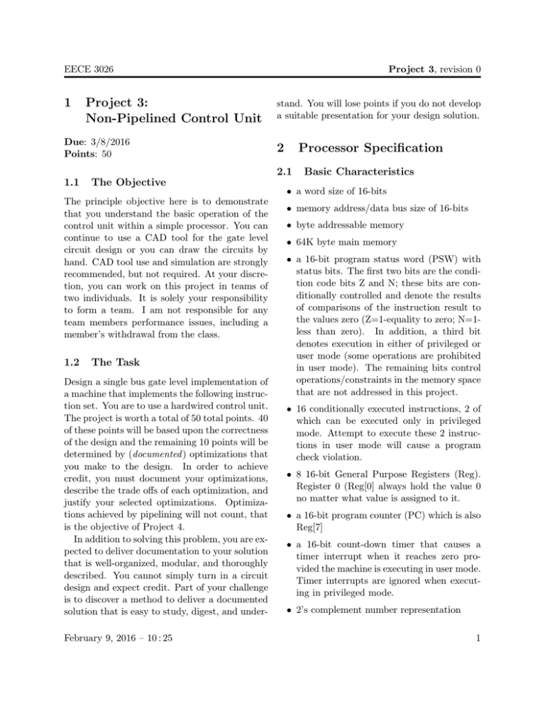
EECE 3026 1 Project 3: Non-Pipelined Control Unit Due: 3/8/2016 Points: 50 Project 3, revision 0 stand. You will lose points if you do not develop a suitable presentation for your design solution. 2 Processor Specification 2.1 1.1 The Objective The principle objective here is to demonstrate that you understand the basic operation of the control unit within a simple processor. You can continue to use a CAD tool for the gate level circuit design or you can draw the circuits by hand. CAD tool use and simulation are strongly recommended, but not required. At your discretion, you can work on this project in teams of two individuals. It is solely your responsibility to form a team. I am not responsible for any team members performance issues, including a member’s withdrawal from the class. 1.2 The Task Design a single bus gate level implementation of a machine that implements the following instruction set. You are to use a hardwired control unit. The project is worth a total of 50 total points. 40 of these points will be based upon the correctness of the design and the remaining 10 points will be determined by (documented ) optimizations that you make to the design. In order to achieve credit, you must document your optimizations, describe the trade offs of each optimization, and justify your selected optimizations. Optimizations achieved by pipelining will not count, that is the objective of Project 4. In addition to solving this problem, you are expected to deliver documentation to your solution that is well-organized, modular, and thoroughly described. You cannot simply turn in a circuit design and expect credit. Part of your challenge is to discover a method to deliver a documented solution that is easy to study, digest, and underFebruary 9, 2016 – 10 : 25 Basic Characteristics • a word size of 16-bits • memory address/data bus size of 16-bits • byte addressable memory • 64K byte main memory • a 16-bit program status word (PSW) with status bits. The first two bits are the condition code bits Z and N; these bits are conditionally controlled and denote the results of comparisons of the instruction result to the values zero (Z=1-equality to zero; N=1less than zero). In addition, a third bit denotes execution in either of privileged or user mode (some operations are prohibited in user mode). The remaining bits control operations/constraints in the memory space that are not addressed in this project. • 16 conditionally executed instructions, 2 of which can be executed only in privileged mode. Attempt to execute these 2 instructions in user mode will cause a program check violation. • 8 16-bit General Purpose Registers (Reg). Register 0 (Reg[0] always hold the value 0 no matter what value is assigned to it. • a 16-bit program counter (PC) which is also Reg[7] • a 16-bit count-down timer that causes a timer interrupt when it reaches zero provided the machine is executing in user mode. Timer interrupts are ignored when executing in privileged mode. • 2’s complement number representation 1 EECE 3026 2.2 Project 3, revision 0 Instruction Format When in user mode (i.e., the PSW privileged bit (P) is not set), only the first 14 instructions All instructions are conditionally executed. This can be executed. All 16 instructions can be exeis described more fully below. In this instruction cuted in privileged mode. Attempting to execute set, there are three instruction formats organized a privileged instruction when in user mode sigas follows: nals a program check violation. Z N Opcode Z N Opcode Z N Opcode 0 2 S Rd Rs1 Rd Short_Offset Long_Offset 6 9 12 Rs2 2.4 15 2.4.1 Exceptions Program Check Violations When in user mode (i.e., the PSW privileged bit (P) is not set), only the first 14 instructions can be executed. All 16 instructions can be executed in privileged mode. Attempting to execute a privileged opcode when in user mode signals a program check violation. A program check vio2.3 Instructions lation causes the machine to swap the PC, and The instruction set consists of 16 instructions PSW as follows: shown in Table 1. The notation GPR[]/MM[] de1. MM[0] = PSW notes respectively the register contents/memory contents. 2. MM[2] = PC All instructions are conditionally executed. 3. PSW = MM[4] The first two bits of each instruction format have 4. PC = MM[6] two bits denoting a condition from the condition codes that governs that instruction’s execution. The first bit relates to the Z condition code and 2.4.2 Timeout the second to the N condition code. When set to There exists a count-down timer in the system 1, the bits control the instruction’s execution by that interrupts execution of instructions when requiring that the corresponding condition code executing in user mode. When this counter in the PSW also be set (if both are “1” in the inreaches zero, it triggers an internal state bit. struction, both must be “1” in the PSW. if both This internal state bit is reset when a new value are “0” in the instruction, no test of the PSW is loaded into the clock (by the CLK instruction). condition codes is performed). Likewise if only A timeout exception interrupt occurs when the one is set, then it becomes the condition evalinternal state bit is set and the control unit is at uated against the corresponding condition code an instruction boundary (between instructions). value in the PSW. The effects of the interrupt are to modify the The condition codes are conditionally set by main memory, PC, and PSW in the following the 3-operand instructions of the first instruction way: format. The instruction bit IR.S determines if the execution of the instruction should set the 1. MM[8] = PSW condition code (1 – Yes, 0 – No). If set, the 2. MM[10] = PC condition code bit (N and Z) should be set based 3. PSW = MM[12] on the value resulting from the operation. Rd/Rs1/Rs2 specify one of the general purpose registers, S controls the setting of the condition codes (described below), and the use of the offset fields is defined in the instruction set definition. February 9, 2016 – 10 : 25 2 EECE 3026 Project 3, revision 0 Name ADD ADDM SUB SUBM AND SHL SHRA OR NOT LD ST BR JSR RTS CLK LPSW Opcode 0 1 2 3 4 5 6 7 8 9 10 11 12 13 14 15 Description GPR[Rd] = GPR[Rs1] + GPR[Rs2] GPR[Rd] = GPR[Rd] + MM[PC + Short Offset] GPR[Rd] = GPR[Rs1] - GPR[Rs2] GPR[Rd] = GPR[Rd] - MM[PC+ Short Offset] GPR[Rd] = GPR[Rs1] and GPR[Rs2] GPR[Rd] = shift left(GPR[Rs1]) by GPR[Rs2]3−0 GPR[Rd] = shift right(GPR[Rs1]) by GPR[Rs2]3−0 GPR[Rd] = GPR[Rs1] or GPR[Rs2] GPR[Rd] = not MM[PC + Short Offset] GPR[Rd] = MM[PC + Short Offset] MM[PC + Short Offset] = GPR[Rd] PC = PC + Long Offset GPR[Rd] = PC; PC = PC + Short Offset PC = GPR[Rd] + Short Offset Set timer to MM[PC + Long Offset] PSW = MM[PC + Long Offset] All uses of Short Offset and Long Offset are sign extended; GPR[Rs2]3−0 denotes the low order 4 bits of the register value; the left shift is logical; and the right shift is arithmetic. Table 1: Instruction and their Semantics 4. PC = MM[14] When executing in privileged mode, the countdown timer has no effect. 3 Restrictions 1. You may use any number of internal registers to hold intermediate values. You must restrict yourself to the single bus paradigm — no point-to-point connections are allowed. 2. You may use a constant ROM in this design provided it contains 8 or fewer constants. You do not have to develop a gate level description of the ROM, but you must provide an informal description of its operation. You may assume that it operates sufficiently February 9, 2016 – 10 : 25 fast to provide data to the bus in the same clock cycle as it is needed. 3. Assume that all memory operations are asynchronous. You do not have to develop a gate level implementation of the main memory; however, you do have to give an informal description of its interface. 4. You must develop gate level descriptions of all components except: multiplexers, demultiplexers, encoders, decoders, and flip-flops. You can use and, or, not, xor, nand, and nor logic gates in your solution. 5. Ignore the details regarding the implementation of the count-down timer and define only its interface. You must however, use the system clock to pulse the count-down timer. 3 EECE 3026 4 Project 3, revision 0 The Report Your report must clearly document your design solution. The documentation should include informal descriptions of the various components in your solution. It should should include the control signals written out in a logical structure that can be meaningfully understood by someone not part of the project team. The synthesis of the control unit circuit should be presented, including the finite state automata and the next state table. There are no limits on the length of the report. Good luck. 5 Change Log Revision 0: 2/9/2016 • Initial Version February 9, 2016 – 10 : 25 4
