A New N-Channel Junction Field-Effect Transistor Embedded in the i
advertisement
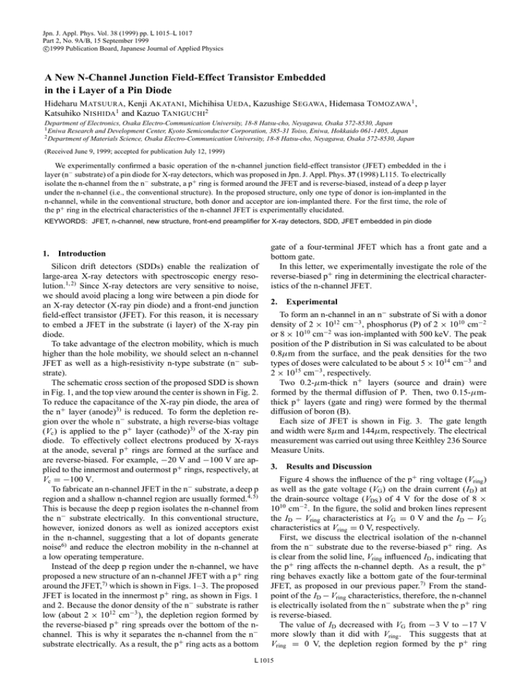
Jpn. J. Appl. Phys. Vol. 38 (1999) pp. L 1015–L 1017 Part 2, No. 9A/B, 15 September 1999 c °1999 Publication Board, Japanese Journal of Applied Physics A New N-Channel Junction Field-Effect Transistor Embedded in the i Layer of a Pin Diode Hideharu M ATSUURA, Kenji A KATANI, Michihisa U EDA, Kazushige S EGAWA, Hidemasa TOMOZAWA1 , Katsuhiko N ISHIDA1 and Kazuo TANIGUCHI2 Department of Electronics, Osaka Electro-Communication University, 18-8 Hatsu-cho, Neyagawa, Osaka 572-8530, Japan 1 Eniwa Research and Development Center, Kyoto Semiconductor Corporation, 385-31 Toiso, Eniwa, Hokkaido 061-1405, Japan 2 Department of Materials Science, Osaka Electro-Communication University, 18-8 Hatsu-cho, Neyagawa, Osaka 572-8530, Japan (Received June 9, 1999; accepted for publication July 12, 1999) We experimentally confirmed a basic operation of the n-channel junction field-effect transistor (JFET) embedded in the i layer (n− substrate) of a pin diode for X-ray detectors, which was proposed in Jpn. J. Appl. Phys. 37 (1998) L115. To electrically isolate the n-channel from the n− substrate, a p+ ring is formed around the JFET and is reverse-biased, instead of a deep p layer under the n-channel (i.e., the conventional structure). In the proposed structure, only one type of donor is ion-implanted in the n-channel, while in the conventional structure, both donor and acceptor are ion-implanted there. For the first time, the role of the p+ ring in the electrical characteristics of the n-channel JFET is experimentally elucidated. KEYWORDS: JFET, n-channel, new structure, front-end preamplifier for X-ray detectors, SDD, JFET embedded in pin diode 1. Introduction Silicon drift detectors (SDDs) enable the realization of large-area X-ray detectors with spectroscopic energy resolution.1, 2) Since X-ray detectors are very sensitive to noise, we should avoid placing a long wire between a pin diode for an X-ray detector (X-ray pin diode) and a front-end junction field-effect transistor (JFET). For this reason, it is necessary to embed a JFET in the substrate (i layer) of the X-ray pin diode. To take advantage of the electron mobility, which is much higher than the hole mobility, we should select an n-channel JFET as well as a high-resistivity n-type substrate (n− substrate). The schematic cross section of the proposed SDD is shown in Fig. 1, and the top view around the center is shown in Fig. 2. To reduce the capacitance of the X-ray pin diode, the area of the n+ layer (anode)3) is reduced. To form the depletion region over the whole n− substrate, a high reverse-bias voltage (Vc ) is applied to the p+ layer (cathode)3) of the X-ray pin diode. To effectively collect electrons produced by X-rays at the anode, several p+ rings are formed at the surface and are reverse-biased. For example, −20 V and −100 V are applied to the innermost and outermost p+ rings, respectively, at Vc = −100 V. To fabricate an n-channel JFET in the n− substrate, a deep p region and a shallow n-channel region are usually formed.4, 5) This is because the deep p region isolates the n-channel from the n− substrate electrically. In this conventional structure, however, ionized donors as well as ionized acceptors exist in the n-channel, suggesting that a lot of dopants generate noise6) and reduce the electron mobility in the n-channel at a low operating temperature. Instead of the deep p region under the n-channel, we have proposed a new structure of an n-channel JFET with a p+ ring around the JFET,7) which is shown in Figs. 1–3. The proposed JFET is located in the innermost p+ ring, as shown in Figs. 1 and 2. Because the donor density of the n− substrate is rather low (about 2 × 1012 cm−3 ), the depletion region formed by the reverse-biased p+ ring spreads over the bottom of the nchannel. This is why it separates the n-channel from the n− substrate electrically. As a result, the p+ ring acts as a bottom gate of a four-terminal JFET which has a front gate and a bottom gate. In this letter, we experimentally investigate the role of the reverse-biased p+ ring in determining the electrical characteristics of the n-channel JFET. 2. Experimental To form an n-channel in an n− substrate of Si with a donor density of 2 × 1012 cm−3 , phosphorus (P) of 2 × 1010 cm−2 or 8 × 1010 cm−2 was ion-implanted with 500 keV. The peak position of the P distribution in Si was calculated to be about 0.8µm from the surface, and the peak densities for the two types of doses were calculated to be about 5 × 1014 cm−3 and 2 × 1015 cm−3 , respectively. Two 0.2-µm-thick n+ layers (source and drain) were formed by the thermal diffusion of P. Then, two 0.15-µmthick p+ layers (gate and ring) were formed by the thermal diffusion of boron (B). Each size of JFET is shown in Fig. 3. The gate length and width were 8µm and 144µm, respectively. The electrical measurement was carried out using three Keithley 236 Source Measure Units. 3. Results and Discussion Figure 4 shows the influence of the p+ ring voltage (Vring ) as well as the gate voltage (VG ) on the drain current (ID ) at the drain-source voltage (VDS ) of 4 V for the dose of 8 × 1010 cm−2 . In the figure, the solid and broken lines represent the ID − Vring characteristics at VG = 0 V and the ID − VG characteristics at Vring = 0 V, respectively. First, we discuss the electrical isolation of the n-channel from the n− substrate due to the reverse-biased p+ ring. As is clear from the solid line, Vring influenced ID , indicating that the p+ ring affects the n-channel depth. As a result, the p+ ring behaves exactly like a bottom gate of the four-terminal JFET, as proposed in our previous paper.7) From the standpoint of the ID − Vring characteristics, therefore, the n-channel is electrically isolated from the n− substrate when the p+ ring is reverse-biased. The value of ID decreased with VG from −3 V to −17 V more slowly than it did with Vring . This suggests that at Vring = 0 V, the depletion region formed by the p+ ring L 1015 L 1016 H. M ATSUURA et al. Jpn. J. Appl. Phys. Vol. 38 (1999) Pt. 2, No. 9A/B Fig. 1. Schematic cross section of the X-ray pin diode with the proposed n-channel JFET. -20 ID [µA] 10 -15 VG [V] -10 -5 0 P : 500 keV, 8x1010 cm-2 VDS = 4 V 5 : VG= 0 V : Vring= 0 V Fig. 2. Schematic top view around the center with the proposed n-channel JFET. 0 -20 -15 -10 Vring [V] -5 0 Fig. 4. Dependence of ID on the reverse bias of the p+ ring (solid line) or the gate (broken line) at VDS = 4 V. Fig. 3. Schematic cross section of the proposed n-channel JFET in the n− substrate. does not spread over the entire bottom area of the n-channel. Since the electronic built-in barrier between the n-channel and the n− substrate is low, ID consists of two types of currents through the n-channel as well as the n− substrate just under the n-channel. On the other hand, at VG < −17 V, ID increased due to the reverse-bias current between the gate and the drain. This is because at VG < −17 V, the gate current (IG ) flowed and IG was the same as ID . Figure 5 shows the ID − VDS characteristics for 11 VG at Vring = −20 V. According to the simulation, the depletion region in the n− substrate spreads over about 100µm at Vring = −20 V. As is clear from the figure, the typical ID − VDS characteristics were obtained, and the saturation of ID appeared clearly, indicating that the pinch-off occurred. Therefore, from the viewpoint of the ID − VDS characteristics also, we have experimentally demonstrated that the reversebiased p+ ring can separate the n-channel from the n− substrate electrically. The electrical characteristics of the JFET for the dose of 2 × 1010 cm−2 were also measured. The pinch-off Vring for the dose of 2 × 1010 cm−2 was about −7 V, while the pinchoff Vring for the dose of 8 × 1010 cm−2 was less than −20 V. Under the conditions of VDS = 4 V, VG = 0 V and Vring = 0 V, ID was in the linear region, and the values of ID were 2.6µA and 11.4µA for the doses of 2×1010 cm−2 and 8×1010 cm−2 , respectively. The ratio of the latter ID to the former ID was 4.4. This ratio is reasonable because in the linear region, ID is proportional to the donor density in the n-channel.8) H. M ATSUURA et al. Jpn. J. Appl. Phys. Vol. 38 (1999) Pt. 2, No. 9A/B 0.15 P : 500 keV, 8x1010 cm-2 Vring= -20 V current JFET. Since the input voltage (Vin ) is around 0 V in the operating condition, the output voltage (Vout ) is around half of the supplied voltage (VCC ). In the saturation region, the small 1Vin can be converted into the large 1Vout . For example, 1Vout /1Vin is estimated to be around 40 at VCC = 8 V using the ID − VDS curve at VG = 0 V shown in Fig. 5. The lower the slope of ID in the saturation region, the more 1Vout /1Vin is enhanced. According to the above discussion, the fabrication of the front-end JFET and the constant-current JFET are in progress. Moreover, in order to confirm the reduction of noise, SDDs with the two types of JFETs are being fabricated. VG [V] 0 -0.1 -0.2 0.1 ID [µA] -0.3 -0.4 -0.5 -0.6 -0.7 -0.8 -0.9 -1.0 0.05 0 Fig. 5. 1 2 3 4 VDS [V] 5 L 1017 4. Conclusion 6 ID − VDS characteristics for 11 VG at Vring = −20 V. We investigated the role of the p+ ring in the n-channel JFET proposed in our previous paper. In the JFET, instead of the deep p region under the n-channel, the p+ ring is located around the n-channel. For the first time, we experimentally proved that the reverse-biased p+ ring can separate the n-channel from the n− substrate electrically and that it acts as a bottom gate of the four-terminal JFET which has a front gate and a bottom gate. Acknowledgements We would like to express our gratitude to Mr. T. Utaka of Rigaku Industrial Corporation for his support during this work. This work is partially supported by Japan Science and Technology Corporation. Fig. 6. Front-end JFET and constant-current JFET: (a) schematic top view and (b) electrical circuit diagram. Since X-ray pin diodes are operated at a low temperature in order to avoid thermal noise, ID should be low in order to avoid generation of heat. On the other hand, when ID is low, it is difficult to obtain high transconductance (gm = ∂ ID /∂ VG ). In order to obtain a high amplification factor, we propose the combination of the front-end JFET and a constant-current JFET in the innermost p+ ring, as shown in Fig. 6, where the sizes of the two JFETs are the same. To obtain a constant current, the gate is connected to the source in the constant- 1) See, for example, Nucl. Instrum. & Methods in Phys. Res. A377 (1996) 346. 2) R. Hartmann, D. Hauff, S. Krisch, P. Lechner, G. Lutz, R. H. Seitz, L. Strüder, G. Bertuccio, L. Fasoli, C. Fiorini, E. Gatti, A. Longoni, E. Pinotti and M. Sampietro: Tech. Dig. Int. Electron Devices Lett. 10 (1989) 91. 3) In the case of detectors for high-energy physics applications, the electrode where electrons or holes are collected is called an anode or a cathode. Therefore, in this letter, the negatively biased p+ layer is referred to as a cathode and the n+ layer is called an anode, although the p+ and n+ layers in a pin diode are usually called an anode and a cathode, respectively. 4) V. Radeka, P. Rehak, S. Rescia, E. Gatti, A. Longoni, M. Sampietro, G. Bertuccio, P. Holl, L. Strüder and J. Kemmer: IEEE Electron Device Lett. 2 (1989) 91. 5) G. Bertuccio, L. Fasoli, C. Fiorini, E. Gatti, A. Longoni, M. Sampietro, D. Hauff, J. Kemmer and R. Richter: Nucl. Instrum. & Methods in Phys. Res. A377 (1996) 352. 6) K. Kandiah and F. B. Whiting: Nucl. Instrum. & Methods in Phys. Res. A326 (1993) 49. 7) H. Matsuura and K. Nishida: Jpn. J. Appl. Phys. 37 (1998) L115. 8) R. F. Pierret: Semiconductor Device Fundamentals (Addison-Wesley, Massachusetts, 1996) p. 540.
