W82M32V-XBX
2Mx32 SRAM 3.3V MULTI-CHIP PACKAGE
FEATURES
Low Power CMOS
Access Times of 12, 15, 17, 20ns
TTL Compatible Inputs and Outputs
Packaging
Fully Static Operation:
2
• 255 PBGA, 25mm x 25mm, 625mm
Organized as 2Mx32
• No clock or refresh required.
Three State Output.
Commercial, Industrial and Military Temperature Ranges
Low Voltage Operation:
* This product is subject to change without notice.
• 3.3V ± 10% Power Supply
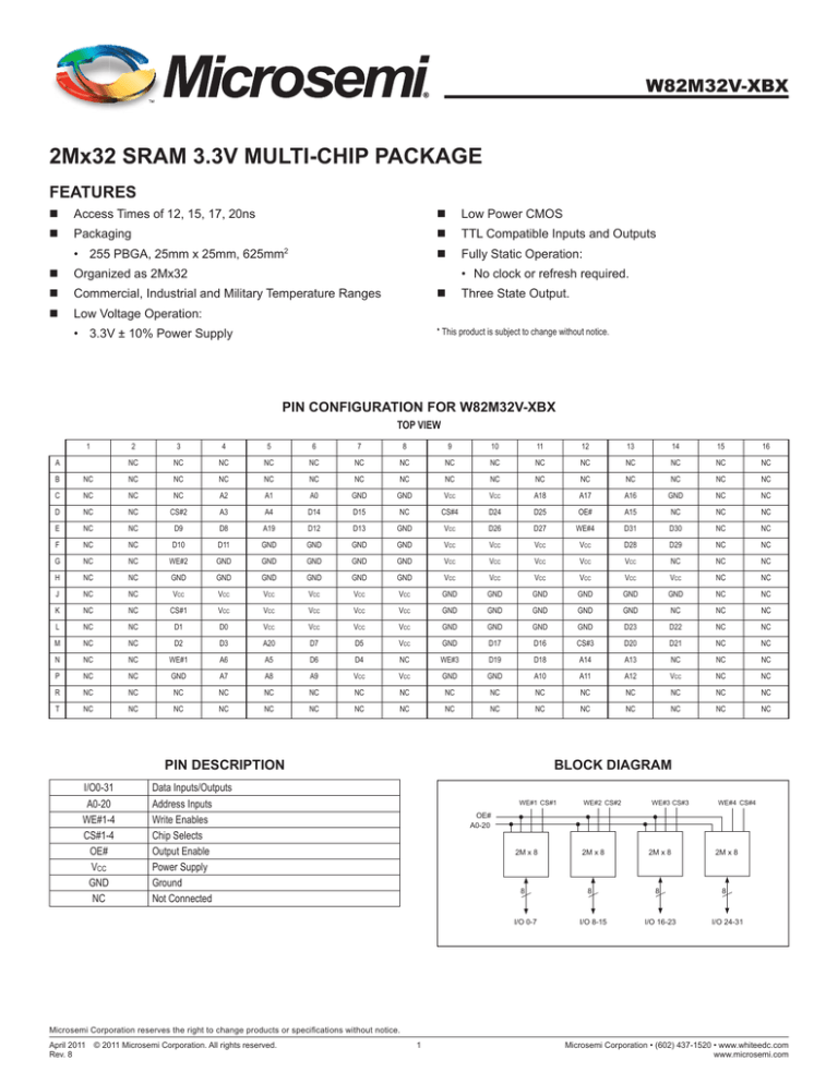
PIN CONFIGURATION FOR W82M32V-XBX
TOP VIEW
1
A
2
3
4
5
6
7
8
9
10
11
12
13
14
15
16
NC
NC
NC
NC
NC
NC
NC
NC
NC
NC
NC
NC
NC
NC
NC
B
NC
NC
NC
NC
NC
NC
NC
NC
NC
NC
NC
NC
NC
NC
NC
NC
C
NC
NC
NC
A2
A1
A0
GND
GND
VCC
VCC
A18
A17
A16
GND
NC
NC
D
NC
NC
CS#2
A3
A4
D14
D15
NC
CS#4
D24
D25
OE#
A15
NC
NC
NC
E
NC
NC
D9
D8
A19
D12
D13
GND
VCC
D26
D27
WE#4
D31
D30
NC
NC
NC
F
NC
NC
D10
D11
GND
GND
GND
GND
VCC
VCC
VCC
VCC
D28
D29
NC
G
NC
NC
WE#2
GND
GND
GND
GND
GND
VCC
VCC
VCC
VCC
VCC
NC
NC
NC
H
NC
NC
GND
GND
GND
GND
GND
GND
VCC
VCC
VCC
VCC
VCC
VCC
NC
NC
NC
J
NC
NC
VCC
VCC
VCC
VCC
VCC
VCC
GND
GND
GND
GND
GND
GND
NC
K
NC
NC
CS#1
VCC
VCC
VCC
VCC
VCC
GND
GND
GND
GND
GND
NC
NC
NC
L
NC
NC
D1
D0
VCC
VCC
VCC
VCC
GND
GND
GND
GND
D23
D22
NC
NC
M
NC
NC
D2
D3
A20
D7
D5
VCC
GND
D17
D16
CS#3
D20
D21
NC
NC
N
NC
NC
WE#1
A6
A5
D6
D4
NC
WE#3
D19
D18
A14
A13
NC
NC
NC
P
NC
NC
GND
A7
A8
A9
VCC
VCC
GND
GND
A10
A11
A12
VCC
NC
NC
R
NC
NC
NC
NC
NC
NC
NC
NC
NC
NC
NC
NC
NC
NC
NC
NC
T
NC
NC
NC
NC
NC
NC
NC
NC
NC
NC
NC
NC
NC
NC
NC
NC
PIN DESCRIPTION
I/O0-31
A0-20
WE#1-4
CS#1-4
OE#
VCC
GND
NC
BLOCK DIAGRAM
Data Inputs/Outputs
Address Inputs
Write Enables
Chip Selects
Output Enable
Power Supply
Ground
Not Connected
WE#1 CS#1
WE#2 CS#2
WE#3 CS#3
WE#4 CS#4
OE#
A0-20
2M x 8
8
I/O 0-7
2M x 8
8
I/O 8-15
2M x 8
8
I/O 16-23
2M x 8
8
I/O 24-31
Microsemi Corporation reserves the right to change products or specifications without notice.
April 2011
Rev. 8
© 2011 Microsemi Corporation. All rights reserved.
1
Microsemi Corporation • (602) 437-1520 • www.whiteedc.com
www.microsemi.com
W82M32V-XBX
ABSOLUTE MAXIMUM RATINGS
Parameter
Operating Temperature
Storage Temperature
Signal Voltage Relative to GND
Junction Temperature
Supply Voltage
Symbol
TA
TSTG
VG
TJ
VCC
Min
-55
-65
-0.5
-0.5
TRUTH TABLE
Max
+125
+150
4.6
150
4.6
Unit
°C
°C
V
°C
V
CS#
H
L
L
L
OE#
X
L
X
H
WE#
X
H
L
H
RECOMMENDED OPERATING CONDITIONS
Parameter
Supply Voltage
Input High Voltage
Input Low Voltage
Symbol
VCC
VIH
VIL
Min
3.0
2.2
-0.3
Max
3.6
VCC + 0.3
+0.8
Mode
Standby
Read
Write
Out Disable
Data I/O
High Z
Data Out
Data In
High Z
Power
Standby
Active
Active
Active
CAPACITANCE
Unit
V
V
V
(TA = +25°C)
Parameter
OE# capacitance
WE#1-4 capacitance
CS#1-4 capacitance
Data I/O capacitance
Address input capacitance
Symbol
COE
CWE
CCS
CI/O
CAD
Conditions
VIN = 0 V, f = 1.0 MHZ
VIN = 0 V, f = 1.0 MHZ
VIN = 0 V, f = 1.0 MHZ
VI/O = 0 V, f = 1.0 MHZ
VIN = 0 V, f = 1.0 MHZ
Max Unit
30
pF
10
pF
10
pF
10
pF
30
pF
This parameter is guaranteed by design but not tested.
DC CHARACTERISTICS
(VCC = 3.3V ± 0.3V, -55°C ≤ TA ≤ 125°C)
Parameter
Input Leakage Current
Output Leakage Current
Operating Supply Current (x 32 Mode)
Standby Current
Output Low Voltage
Output High Voltage
Sym
ILI
ILO
ICC x 32
ISB
VOL
VOH
Conditions
VIN = GND to VCC
CS# = VIH, OE# = VIH, VOUT = GND to VCC
CS# = VIL, OE# = VIH, f = 5MHZ, VCC = 3.6V
CS# = VIH, OE# = VIH, f = 5MHZ, VCC = 3.6V
IOL = 8mA
IOH = -4.0mA
Min
2.4
Max
10
10
1100
200
0.4
Units
μA
μA
mA
mA
V
V
NOTE: DC test conditions: VIH = VCC -0.3V, VIL = 0.3V.
NOTE: Contact factory for low power option.
Microsemi Corporation reserves the right to change products or specifications without notice.
April 2011
Rev. 8
© 2011 Microsemi Corporation. All rights reserved.
2
Microsemi Corporation • (602) 437-1520 • www.whiteedc.com
www.microsemi.com
W82M32V-XBX
AC CHARACTERISTICS
(VCC = 3.3V, -55°C ≤ TA ≤ +125°C)
-12
Parameter
Symbol
Read Cycle
Read Cycle Time
Address Access Time
Output Hold from Address Change
Chip Select Access Time
Output Enable to Output Valid
Chip Select to Output in Low Z
Output Enable to Output in Low Z
Chip Disable to Output in High Z
Output Disable to Output in High Z
tRC
tAA
tOH
tACS
tOE
tCLZ1
tOLZ1
tCHZ1
tOHZ1
Min
-15
Max
Min
12
-17
Max
15
Min
Max
17
12
3
3
1
17
8
3
1
7
7
20
3
15
8
3
1
Max
17
3
12
7
Min
20
15
3
-20
20
10
3
1
8
8
8
8
10
10
Units
ns
ns
ns
ns
ns
ns
ns
ns
ns.
1. This parameter is guaranteed by design but not tested
AC CHARACTERISTICS
(VCC = 3.3V, -55°C ≤ TA ≤ +125°C)
Parameter
Symbol
-12
Min
Write Cycle
Write Cycle Time
Chip Select to End of Write
Address Valid to End of Write
Data Valid to End of Write
Write Pulse Width
Address Setup Time
Address Hold Time
Output Active from End of Write
Write Enable to Output in High Z
Data Hold Time
tWC
tCW
tAW
tDW
tWP
tAS
tAH
tOW1
tWHZ1
tDH
-15
Max
Min
12
10
10
8
10
0
0
2
-17
Max
15
12
12
9
12
0
0
2
7
Min
17
12
12
9
14
0
0
3
0
Min
Units
Max
20
14
14
10
14
0
0
3
8
0
-20
Max
8
0
9
0
ns
ns
ns
ns
ns
ns
ns
ns
ns
ns
1. This parameter is guaranteed by design but not tested
AC TEST CIRCUIT
AC TEST CONDITIONS
Parameter
Input Pulse Levels
Input Rise and Fall
Input and Output Reference Level
Output Timing Reference Level
IOL
Current Source
D.U.T.
Unit
V
ns
V
V
NOTES:
VZ is programmable from -2V to +7V.
IOL & IOH programmable from 0 to 16mA.
Tester Impedance Z0 = 75 W.
VZ is typically the midpoint of VOH and VOL.
IOL & IOH are adjusted to simulate a typical resistive load circuit. ATE tester includes jig capacitance.
VZ 1.5V
(Bipolar Supply)
CEFF = 50pf
Typ
VIL = 0, VIH = 2.5
5
1.5
1.5
IOH
Current Source
Microsemi Corporation reserves the right to change products or specifications without notice.
April 2011
Rev. 8
© 2011 Microsemi Corporation. All rights reserved.
3
Microsemi Corporation • (602) 437-1520 • www.whiteedc.com
www.microsemi.com
W82M32V-XBX
TIMING WAVEFORM – READ CYCLE
tRC
ADDRESS
tRC
tAA
ADDRESS
CS#
tAA
tOH
DATA I/O
tCHZ
tACS
tCLZ
PREVIOUS DATA VALID
OE#
DATA VALID
tOE
tOLZ
DATA I/O
READ CYCLE 1 (CS# = OE# = VIL, WE# = VIH)
tOHZ
DATA VALID
HIGH IMPEDANCE
READ CYCLE 2 (WE# = VIH)
WRITE CYCLE – WE# CONTROLLED
tWC
ADDRESS
tAW
tAH
tCW
CS#
tAS
tWP
WE#
tOW
tWHZ
tDW
DATA I/O
tDH
DATA VALID
WRITE CYCLE 1, WE# CONTROLLED
WRITE CYCLE – CS# CONTROLLED
tWC
ADDRESS
tAS
tAW
tAH
tCW
CS#
tWP
WE#
tDW
DATA I/O
tDH
DATA VALID
WRITE CYCLE 1, WE# CONTROLLED
Microsemi Corporation reserves the right to change products or specifications without notice.
April 2011
Rev. 8
© 2011 Microsemi Corporation. All rights reserved.
4
Microsemi Corporation • (602) 437-1520 • www.whiteedc.com
www.microsemi.com
W82M32V-XBX
PACKAGE 781 – 255 BALL GRID ARRAY
BOTTOM VIEW
16 15 14 13 12 11 10 9
8
7
6
5
4
3
2
1
255x Ø0.762(0.030) NOM
A
B
C
19.05 (0.750) NOM
25.1 (0.988) MAX
D
E
F
G
H
1.27
(0.050)
NOM
J
K
L
M
N
P
R
T
0.69
(0.027)
NOM
1.27 (0.050) NOM
19.05 (0.750) NOM
2.22 (0.087) MAX
25.1 (0.955) MAX
ALL LINEAR DIMENSIONS ARE MILLIMETERS AND PARENTHETICALLY IN INCHES
Microsemi Corporation reserves the right to change products or specifications without notice.
April 2011
Rev. 8
© 2011 Microsemi Corporation. All rights reserved.
5
Microsemi Corporation • (602) 437-1520 • www.whiteedc.com
www.microsemi.com
W82M32V-XBX
ORDERING INFORMATION
W 8 2M 32 V - XX X X
MICROSEMI CORPORATION
SRAM
ORGANIZATION, 2Mx32
User configurable as 4Mx16 or 8Mx8
Low Voltage Supply 3.3V ± 10%
ACCESS TIME (ns)
PACKAGE TYPE:
B = 25mm x 25mm, 255 PBGA
DEVICE GRADE:
M = Military
I = Industrial
C = Commercial
-55°C to +125°C
-40°C to +85°C
0°C to +70°C
Microsemi Corporation reserves the right to change products or specifications without notice.
April 2011
Rev. 8
© 2011 Microsemi Corporation. All rights reserved.
6
Microsemi Corporation • (602) 437-1520 • www.whiteedc.com
www.microsemi.com
W82M32V-XBX
Document Title
2M x 32 Asynchronous SRAM
Revision History
Rev #
History
Release Date
Status
Rev 0
Initial Release
July 2002
Advanced
Rev 1
Changes
1.1 Add AC/DC Electricals & Timing Diagrams (Pg. 1-7)
1.2 Change Pinout to full 255 (16x16) array
1.3 Change Package Dimension to full 255 (16x16) array
October 2002
Advanced
Rev 2
Changes (Pg.1,5,6,7)
2.1 Change package dimension from 27mm square to 25mm square
2.2 Change package height from 2.20mm to 2.70mm Max
May 2002
Advanced
Rev 3
Changes (Pg.1,5,7)
3.1 Change package mechanical drawing to new format.
November 2003
Advanced
Rev 4
Changes (Pg.1,7)
4.1 Change status to preliminary.
May 2004
Preliminary
Rev 5
Changes (Pg. 1, 7)
5.1 Change status to Final
April 2006
Final
Rev 6
Change (Pg. 5)
6.1 Change max height dimension to 2.21mm/0.087in
October 2008
Final
Rev 7
Change (Pg. 5)
7.1 Change standby current (ISB) from 400 to 200mA
May 2009
Final
Rev 8
Changes (Pg. 1-7)
April 2011
Final
8.1 Change document layout from White Electronic Designs to Microsemi
Microsemi Corporation reserves the right to change products or specifications without notice.
April 2011
Rev. 8
© 2011 Microsemi Corporation. All rights reserved.
7
Microsemi Corporation • (602) 437-1520 • www.whiteedc.com
www.microsemi.com


![Iin Vin Vin and Iin are the values given in [Series Impedance] Vload](http://s2.studylib.net/store/data/018206929_1-d327defc9b9e133751f2a98335f9c6fb-300x300.png)
