Circuit Note
CN-0193
Devices Connected/Referenced
Circuits from the Lab™ tested circuit designs address
common design challenges and are engineered for
quick and easy system integration. For more information
and/or support, visit www.analog.com/CN0193.
AD5504
Quad, 12-Bit, 30 V/60 V DAC
ADP1613
650 kHz /1.3 MHz Step-Up PWM
DC-to-DC Switching Converter
High Voltage (30 V) DAC Powered from a Low Voltage (3 V) Supply Generates
Tuning Signals for Antennas and Filters
EVALUATION AND DESIGN SUPPORT
in being able to tune these applications—for example,
compensating for component tolerance errors, fine tuning the
cutoff frequency of a filter, or network impedance matching for
tunable antennas.
CIRCUIT FUNCTION AND BENEFITS
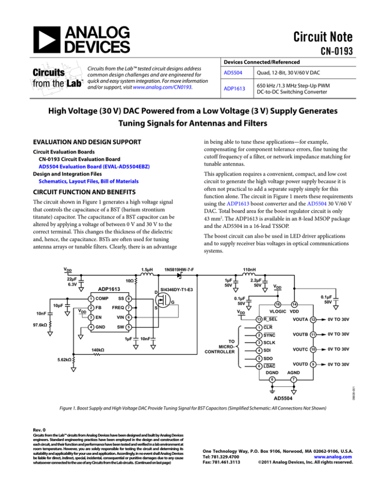
The circuit shown in Figure 1 generates a high voltage signal
that controls the capacitance of a BST (barium strontium
titanate) capacitor. The capacitance of a BST capacitor can be
altered by applying a voltage of between 0 V and 30 V to the
correct terminal. This changes the thickness of the dielectric
and, hence, the capacitance. BSTs are often used for tuning
antenna arrays or tunable filters. Clearly, there is an advantage
VDD
1.5µH
22µF
6.3V
1
10pF
10nF
97.6kΩ
VDD
COMP
D
SS 8
2
FB
FREQ 7
3
EN
VIN 6
4
GND
SW 5
1µF
The boost circuit can also be used in LED driver applications
and to supply receiver bias voltages in optical communications
systems.
110nH
1N5819HW-7-F
10Ω
ADP1613
This application requires a convenient, compact, and low cost
circuit to generate the high voltage power supply because it is
often not practical to add a separate supply simply for this
function alone. The circuit in Figure 1 meets these requirements
using the ADP1613 boost converter and the AD5504 30 V/60 V
DAC. Total board area for the boost regulator circuit is only
43 mm2. The ADP1613 is available in an 8-lead MSOP package
and the AD5504 in a 16-lead TSSOP.
S
SI4346DY-T1-E3
G
10nF
140kΩ
5.62kΩ
1µF
50V
2.2µF
50V
VDD
0.1µF
50V
16
VDD
TO
MICROCONTROLLER
14
0.1µF
50V
VLOGIC VDD
13
R_SEL
1
CLR
2
SYNC
3
SCLK
4
SDI
5
SDO
6
LDAC
VOUTA 12
0V TO 30V
VOUTB 11
0V TO 30V
VOUTC 10
0V TO 30V
VOUTD 9
0V TO 30V
DGND
AGND
6
7
AD5504
09608-001
Circuit Evaluation Boards
CN-0193 Circuit Evaluation Board
AD5504 Evaluation Board (EVAL-AD5504EBZ)
Design and Integration Files
Schematics, Layout Files, Bill of Materials
Figure 1. Boost Supply and High Voltage DAC Provide Tuning Signal for BST Capacitors (Simplified Schematic: All Connections Not Shown)
Rev. 0
Circuits from the Lab™ circuits from Analog Devices have been designed and built by Analog Devices
engineers. Standard engineering practices have been employed in the design and construction of
each circuit, and their function and performance have been tested and verified in a lab environment at
room temperature. However, you are solely responsible for testing the circuit and determining its
suitability and applicability for your use and application. Accordingly, in no event shall Analog Devices
be liable for direct, indirect, special, incidental, consequential or punitive damages due to any cause
whatsoever connected to the use of any Circuits from the Lab circuits. (Continued on last page)
One Technology Way, P.O. Box 9106, Norwood, MA 02062-9106, U.S.A.
Tel: 781.329.4700
www.analog.com
Fax: 781.461.3113
©2011 Analog Devices, Inc. All rights reserved.
Circuit Note
CN-0193
CIRCUIT DESCRIPTION
changed by writing to the appropriate DAC registers via the
serial interface. The DACs can be updated simultaneously by
pulsing the Load DAC (LDAC) pin low, thus allowing for all
four BST capacitors to be changed at the same time.
The circuit has a 3 V (VDD) power supply available, and the BST
capacitors require voltages in excess of 20 V for full control. The
two main circuit blocks are the ADP1613 step-up switching
converter and the AD5504 high voltage DAC. The circuit
diagram is shown in Figure 1.
Using the circuit shown in Figure 1, it is possible to generate
DAC output voltages up to 30 V. The output voltages are used to
set the bias voltage for BST capacitors, which, in turn, adjust the
antenna response. Figure 2 shows the equivalent circuit of a BST
capacitor used as a tunable matching network, and Figure 3
shows the transfer function of the BST capacitance as a function
of bias voltage and the resulting antenna response. More
information on BST capacitors can be found at www.agilerf.com.
The ADP1613 is a step-up dc-to-dc switching converter with an
integrated power switch capable of providing an output as high
as 20 V. Using additional external components, higher voltages
can be achieved. The ADP1613 has an adjustable soft start
function to prevent inrush current when the device is enabled.
The pin-selectable switching frequency and PWM current
mode architecture allows easy noise filtering and yields
excellent transient response. The components connected
around the ADP1613 generate a 32 V output from a 3 V input.
AD5504 OUTPUT
(CONTROL VOLTAGE)
BST
CAP
09608-002
+
BST
CAP
In any circuit where accuracy is important, it is important to
consider the power supply and ground return layout on the
board. The printed circuit board (PCB) containing the circuit
should have separate analog and digital sections. If the circuit is
used in a system where other devices require an AGND-toDGND connection, the connection should be made at one
point only. This ground point should be as close as possible to
the AD5504. The circuit should be constructed on a multilayer
VOLTAGE VARIABLE CAPACITANCE
ANTENNA RESPONSE
0
1
–4
–8
0.8
3
–12
S11 (dB)
2
0.6
–16
1
–20
3
0.4
2
–24
0.2
0
SEE ANTENNA RESPONSE #1
SEE ANTENNA RESPONSE #2
SEE ANTENNA RESPONSE #3
0
5
10
15
ANTENNA RESPONSE #1
ANTENNA RESPONSE #2
ANTENNA RESPONSE #3
–28
20
–32
780
BIAS VOLTAGE (V)
800
820
840
860
880
900
FREQUENCY (MHz)
Figure 3. Bias Voltage vs. BST Capacitance, and Resulting Antenna Response
Rev. 0 | Page 2 of 3
920
940
960
980
09608-003
NORMALIZED CAPACITANCE
DC
BLOCK
4.62nH
Figure 2. BST Capacitor Equivalent Circuit
The 32 V output from the ADP1613 is used as the power supply
for the AD5504. The AD5504 is a quad channel, 12 bit DAC
capable of an output voltage up to 60 V. The full-scale output of
the AD5504 is determined by the state of the R_SEL pin. In this
application, R_SEL is connected to VDD, selecting a full-scale
output of 30 V. The AD5504 is controlled by a serial interface,
which is compatible with 3 V logic. The DAC outputs are
1.0
DC
BLOCK
RF SIGNAL
The ADIsimPower design file includes the bill of material,
detailed schematic, bode plots, efficiency plots, transient
response, as well as a suggested board layout.
1.2
ANTENNA
+
The ADIsimPower™ design tool provides an easy way for
designers to determine the appropriate components based on
input and output requirements. The design of the ADP1613
circuit shown in Figure 1 uses the "lowest cost" option of
ADIsimPower with an input voltage of 3 V, output voltage of 32
V, and a load current of 40 mA. The design can be downloaded
at www.analog.com/CN0193-PowerDesign.
Circuit Note
CN-0193
CIRCUIT EVALUATION AND TEST
PCB with a large area ground plane layer and a power plane
layer. See MT-031 Tutorial for more discussion on layout and
grounding.
The power supply to the AD5504 should be bypassed with
10 μF and 0.1 μF capacitors. The capacitors should be as
physically close as possible to the device, with the 0.1 μF
capacitor ideally right up against the device. The 10 μF
capacitor should be either the tantalum bead type or ceramic
type. It is important that the 0.1 μF capacitor have low effective
series resistance (ESR) and low effective series inductance
(ESL), such as is typical of common ceramic types of capacitors.
This 0.1 μF capacitor provides a low impedance path to ground
for high frequencies caused by transient currents due to internal
logic switching. See MT-101 Tutorial for more details on proper
decoupling techniques.
The power supply line should have as large a trace as possible to
provide a low impedance path and reduce glitch effects on the
supply line. Clocks and other fast switching digital signals
should be shielded from other parts of the board by digital
ground.
The circuit of Figure 1 is tested by applying a 3 V power supply
to VDD. This creates a 32 V supply for the AD5504 (measurable
on Pin 14) and also supplies the VLOGIC supply for the
AD5504. A microcontroller, DSP, or FPGA is used to provide
the appropriate digital interface signals to the AD5504.
For normal operation CLR should be high. The SYNC , SCLK,
and SDATA lines should be operated as described in the
AD5504 data sheet to write data to the various registers of the
AD5504. When data is written to a DAC register with LDAC
low, the appropriate output will update immediately. When data
is written to a DAC register with LDAC high, the DAC output
will remain at its current value until LDAC is pulsed low.
LEARN MORE
CN0193 Design Support Package:
http://www.analog.com/CN0193-DesignSupport
ADIsimPower Design File for CN0193:
http://www.analog.com/CN0193-PowerDesign
The ADIsimPower design file shows a recommended layout for
the ADP1613 portion of the circuit. The file can be downloaded
at www.analog.com/CN0193-PowerDesign. A complete
design support package for this circuit note can be found at
www.analog.com/CN0193-DesignSupport.
Kavanagh, Ken. "Boost Supply and High-Voltage DAC Provide
Tuning Signal for Antennas and Filters," Analog Dialogue,
44-12 Back Burner, December 2010.
COMMON VARIATIONS
MT-031 Tutorial, Grounding Data Converters and Solving the
Mystery of "AGND" and "DGND," Analog Devices.
Other boost regulators can be substituted, depending on system
requirements. Refer to the ADIsimPower™ design tool for
details.
The AD5501 is a single channel version of the AD5504.
BST Capacitors: www.agilerf.com
ADIsimPower™ Design Tool, Analog Devices.
MT-101 Tutorial, Decoupling Techniques, Analog Devices.
Data Sheets and Evaluation Boards
AD5504 Data Sheet
ADP1613 Data Sheet
AD5504 Evaluation Board
ADP1613 Evaluation Board
REVISION HISTORY
1/11—Revision 0: Initial Version
(Continued from first page) Circuits from the Lab circuits are intended only for use with Analog Devices products and are the intellectual property of Analog Devices or its licensors. While you
may use the Circuits from the Lab circuits in the design of your product, no other license is granted by implication or otherwise under any patents or other intellectual property by
application or use of the Circuits from the Lab circuits. Information furnished by Analog Devices is believed to be accurate and reliable. However, "Circuits from the Lab" are supplied "as is"
and without warranties of any kind, express, implied, or statutory including, but not limited to, any implied warranty of merchantability, noninfringement or fitness for a particular
purpose and no responsibility is assumed by Analog Devices for their use, nor for any infringements of patents or other rights of third parties that may result from their use. Analog Devices
reserves the right to change any Circuits from the Lab circuits at any time without notice but is under no obligation to do so.
©2011 Analog Devices, Inc. All rights reserved. Trademarks and
registered trademarks are the property of their respective owners.
CN09608-0-1/11(0)
Rev. 0 | Page 3 of 3


