SG1532
Precision General - Purpose Regulator
Description
This monolithic integrated circuit is a versatile, general-purpose
voltage regulator designed as a substantially improved
replacement for the popular SG723 device. The SG1532 series
regulators retain all the versatility of the SG723 but have the
added benefits of operation. The SG1532 series have input
voltages as low as 4.5 V and as high as 50 V, a low noise, low
voltage reference temperature compensated, low threshold
current limiting and protective circuits which include thermal
shutdown and independent current limiting of both the reference
and output voltages. A separate remote shutdown terminal is
included. In the dual-in-line package an open collector output is
available for low input-output differential applications.
These devices are available in a hermetic 14-pin CERDIP. The
SG1532 is rated for operation over the ambient temperature
range of -55°C to 125°C.
Features
Input Voltage Range of 4.5 V to 50 V
2.5 V Low Noise Reference
Independent Shutdown Terminal
Improved Line and Load Regulation
80 mV Current Limit Sense Voltage
Fully Protected Including Thermal Shutdown
Useful Output Current to 150 mA
High Reliability Features
Available to MIL-STD-883, ¶ 1.2.1
Available to DSCC
– Standard Microcircuit Drawing (SMD)
MSC-AMS level “S” Processing Available
www.microsemi.com
© 2015 Microsemi Corporation
1
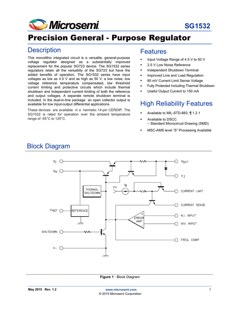
Block Diagram
Figure 1 · Block Diagram
May 2015 Rev. 1.2
Absolute Maximum Ratings (Note 1)
Pulse (50 ms) Input Voltage from VIN to V- ....................... 50 V
Continuous Input Voltage from VIN to V-............................ 40 V
Input to Output Voltage Differential................................... 40 V
Maximum Output Current ........................................... 250 mA
Current from VZ ............................................................ 100 mA
Current from VREF..........................................................
25 mA
Operating Junction Temperature
Storage Temperature Range .......................... -65°C to 150°C
300°C
Lead Temperature (Soldering, 10s) ............................
Note 1. Exceeding these ratings could cause damage to the device.
Thermal Data
J Package:
Thermal Resistance-Junction to Case, θJC ................... 30°C/W
Thermal Resistance-Junction to Ambient, θJA .............. 80°C/W
Note A. Junction Temperature Calculation: TJ = TA + (PD x θJA).
Note B. The above numbers for θJC are maximums for the limiting
thermal resistance of the package in a standard
mounting configuration. The θJA numbers are meant to
be guidelines for the thermal performance of the device/
pc-board system. All of the above assume no ambient
airflow.
Recommended Operating Conditions (Note 2)
Input Voltage Range
SG1532 ................................................................. 5 V to 45 V
Output Current Range ....................................... 1 mA to 100 mA
Reference Current ........................................................ 5 mA
Zener Current ................................................................ 20 mA
Operating Ambient Temperature Range
SG1532 ........................................................ -55°C to 125°C
Note 2. Range over which the device is functional.
Electrical Characteristics
(Unless otherwise specified, these specifications apply over the operating ambient temperature for SG1532 with -55°C ≤ TA ≤ 125°C, VIN = 10 V,
VOUT = 5 V, and IOUT = 1 mA. Low duty cycle pulse testing techniques are used which maintains junction and case temperatures equal to the ambient
temperature.)
Parameter
Test Conditions
Input Voltage Range
TA = 25°C
Output Voltage Range
Max Output Current
Min (VIN - VOUT)
Reference Voltage
RSC = 0, VOUT = 0, TA = 25°C
IOUT = 100 mA, TA = 25°C
TA = 25°C
Temperature Stability (Note 4)
Ref Short Circuit Current
Line Regulation (Note 3)
Load Regulation (Note 3)
Current Limit Sense Voltage
Shutdown Voltage Threshold
Shutdown Source Current
Zener Voltage
Standby Current
Error Amplifier Offset Voltage
Error Amplifier Input Bias Current
VREF = 0, TA = 25°C
8 V ≤ VIN ≤ 40 V
8 V ≤ VIN ≤ 20 V, IOUT = 25 mA
1 mA ≤ IOUT ≤ 25 mA
1 mA ≤ IOUT ≤ 100 mA
RSC = 100 Ω, VOUT = 0 V
VOUT = high
IOUT = 10 mA
VIN = 40 V
2
Min.
4.5
4.7
2.0
2.40
2.35
0.06
0.40
100
6.0
SG1532
Typ.
175
1.7
2.50
0.005
15
0.005
0.01
0.002
0.002
0.08
0.70
200
6.4
2.5
2.0
4.0
Max.
50
50
38
250
2.0
2.60
2.65
0.015
25
0.01
0.02
0.004
0.005
0.10
1.0
300
7.2
3.5
10
15
Units
V
V
V
mA
V
V
V
%/°C
mA
%/V
%/V
%/mA
%/mA
V
V
µA
V
mA
mV
µA
Electrical Characteristics (Continued)
Test Conditions
Parameter
Open Loop Gain
Ripple Rejection
Output Noise (Note 4)
Long Term Stability (Note 4)
Thermal Shutdown (Note 4)
SG1532
Typ.
68
66
50
0.3
175
Min.
66
TA = 25°C
f = 120 Hz, TA = 25°C
10 Hz ≤ f ≤ 100 kHz, TA = 25°C
VIN = 30 V, TA = 125°C
Units
Max.
dB
dB
µVRMS
%/khr
°C
1.0
Note 3. Applies for constant junction temperature. Temperature drift effects must be taken into account separately when the unit is operating under
conditions of high dissipation.
Note 4. These parameters, although guaranteed, are not tested in production.
Characteristics Curves
5V
100 mV
Figure 2. Standby Current
Figure 3. Minimum Input-Output Voltage
10 V
5V
10 Ω
10 V
5V
mA
pF
10
Figure 4. Current Limiting
100
1k
10 k
100 k
Figure 5. Ripple Rejection
3
1M
Characteristics Curves (Continued)
V
V
mA
V
1000 pF
V
mA
V
pF
1000 pF
mA
100
1k
10 k
100 k
1M
Figure 6. Frequency Response
Figure 7. Transient Response
Application Information
2k
1.5 k
510 Ω
1000 pF
1000 pF
Figure 8. 90% Efficient Linear Regulator
Output Voltage = 5 V
Min (VIN-VOUT) at 2 A = 0.4 V
Load Reg 0-2 A = 20 mV
Figure 9. High Current Regulator with Foldback
Current Limiting and Remote Shutdown
Max Output Current = 3 A
Line Reg 6-30 V = 10 mV
Output Voltage = 5 V
Max Output Current = 8 A
Min VIN at No Load = 6.9 V
Min VIN at 5 A = 8.2 V
Line Reg 10-30 V = 3 mV
Load Reg 0-5 A = 17 mV
Short Circuit Current = 1.8 A
Notes:
Note:
1. For output voltages above 8 V and load currents which
allow PNP base current to be limited to 25 mA, the
internal zener may be used, eliminating the need for the
two external diodes and the divider on VREF .
* 100 Ω surge limiting resistor should be used for
output voltages above 8 V.
2. RSC can be eliminated if the 200 mA current limit on VOUT
is adequate. Overall current limiting is dependent
upon PNP Beta. For greater accuracy, load currrent
may be sensed in the ground line.
4
Application Information (Continued)
Figure 10. High Efficiency Low Voltage Regulator
Output Voltage = 5 V
Max Output Current = 9 A
Min VIN at 5 A = 7.0 V
Figure 11. Basic Low Current Regulator
R
VOUT = VREF 1+ 1
R2
Line Reg 7-20 V = 10 mV
Load Reg 0-5 A = 25 mV
Constant Current Limiting
Sense Voltage
RSC
R1 R2
R3 = R +R
1
2
ISC =
CC = 1000 pF
IOUT ≤ 100 mA
Connection Diagrams and Ordering Information (See Notes Below)
Package
Part Number
14-PIN CERAMIC DIP
J - PACKAGE
SG1532J-883B
SG1532J-DESC
SG1532J
Ambient
Temperature Range
-55°C to 125°C
-55°C to 125°C
-55°C to 125°C
Note 1. Contact factory for JAN product availability.
2. All packages are viewed from the top.
5
Connection Diagram
N.C.
CURRENT LIMIT
1
14
2
13
CURRENT SENSE
INVERTING INPUT
NON-INVERTING INPUT
3
12
4
11
5
10
VREF
V-
6
9
7
8
N.C.
FREQ. COMPENSATION
VIN
VC
VOUT
VZ
SHUTDOWN
Package Outline Dimensions
Controlling dimensions are in inches, metric equivalents are shown for general information.
D
DIM
8
14
A
b
b2
c
D
E
e
eA
H
L
α
Q
E
1
7
Q
eA
Q A
b2
c
L
H
e
MILLIMETERS
MIN
MAX
5.08
0.38
0.51
1.04
1.65
0.20
0.38
19.30
19.94
5.59
7.11
2.54 BSC
7.37
7.87
0.63
1.78
3.18
5.08
15°
0.51
1.02
INCHES
MIN
MAX
0.200
0.015
0.020
0.045
0.065
0.008
0.015
0.760
0.785
0.220
0.280
0.100 BSC
0.290
0.310
0.025
0.070
0.125
0.200
15°
0.020
0.040
Note:
b
α
Dimensions do not include protrusions; these shall
not exceed 0.155 mm (.006”) on any side. Lead
dimension shall not include solder coverage.
Figure 12 · J 14-Pin Ceramic Dip Package Dimensions
6
Microsemi Corporation (MSCC) offers a comprehensive portfolio of semiconductor and system
solutions for communications, defense & security, aerospace and industrial markets.
Products include high-performance and radiation-hardened analog mixed-signal integrated
circuits, FPGAs, SoCs and ASICs; power management products; timing and synchronization
devices and precise time solutions, setting the world's standard for time; voice processing
devices; RF solutions; discrete components; security technologies and scalable anti-tamper
products; Ethernet solutions; Power-over-Ethernet ICs and midspans; as well as custom
design capabilities and services. Microsemi is headquartered in Aliso Viejo, Calif., and has
approximately 3,600 employees globally. Learn more at www.microsemi.com.
Microsemi Corporate Headquarters
One Enterprise, Aliso Viejo,
CA 92656 USA
Within the USA: +1 (800) 713-4113
Outside the USA: +1 (949) 380-6100
Sales: +1 (949) 380-6136
Fax: +1 (949) 215-4996
E-mail: sales.support@microsemi.com
© 2015 Microsemi Corporation. All
rights reserved. Microsemi and the
Microsemi logo are trademarks of
Microsemi Corporation. All other
trademarks and service marks are the
property of their respective owners.
Microsemi makes no warranty, representation, or guarantee regarding the information contained herein or
the suitability of its products and services for any particular purpose, nor does Microsemi assume any
liability whatsoever arising out of the application or use of any product or circuit. The products sold
hereunder and any other products sold by Microsemi have been subject to limited testing and should not
be used in conjunction with mission-critical equipment or applications. Any performance specifications are
believed to be reliable but are not verified, and Buyer must conduct and complete all performance and
other testing of the products, alone and together with, or installed in, any end-products. Buyer shall not rely
on any data and performance specifications or parameters provided by Microsemi. It is the Buyer's
responsibility to independently determine suitability of any products and to test and verify the same. The
information provided by Microsemi hereunder is provided "as is, where is" and with all faults, and the entire
risk associated with such information is entirely with the Buyer. Microsemi does not grant, explicitly or
implicitly, to any party any patent rights, licenses, or any other IP rights, whether with regard to such
information itself or anything described by such information. Information provided in this document is
proprietary to Microsemi, and Microsemi reserves the right to make any changes to the information in this
document or to any products and services at any time without notice.
SG1532-1.2/05.15


