HSMS-2700, 2702, 270B, 270C
High Performance Schottky Diode for
Transient Suppression
Data Sheet
Description
Features
The HSMS-2700 series of Schottky diodes, commonly
referred to as clipping /clamping diodes, are optimal
for circuit and waveshape preservation applications
with high speed switching. Ultra-low series resistance,
R S, makes them ideal for protecting sensitive circuit
elements against higher current transients carried on
data lines. With picosecond switching, the HSMS-270x
can respond to noise spikes with rise times as fast as
1 ns. Low capacitance minimizes waveshape loss that
causes signal degradation.
• Ultra-low Series Resistance for Higher Current Handling
• Picosecond Switching
• Low Capacitance
• Lead-free Option Available
Applications
RF and computer designs that require circuit protection, high-speed switching, and voltage clamping.
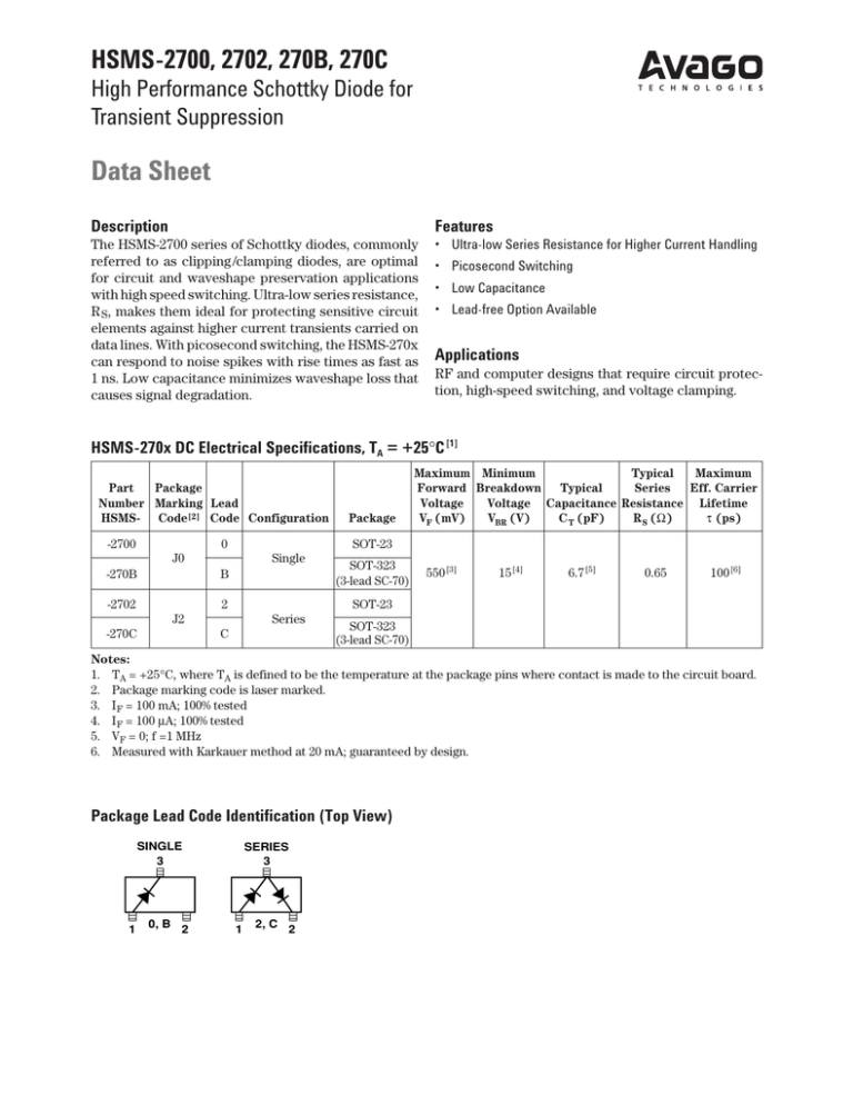
HSMS-270x DC Electrical Specifications, TA = +25°C [1]
Part
Package
Number Marking Lead
HSMS- Code [2] Code Configuration
-2700
0
SOT-23
J0
-270B
Single
B
-2702
2
SOT-323
(3-lead SC-70)
550 [3]
15 [4]
6.7 [5]
0.65
100 [6]
SOT-23
J2
-270C
Package
Maximum Minimum
Typical
Maximum
Forward Breakdown
Typical
Series
Eff. Carrier
Voltage
Voltage Capacitance Resistance Lifetime
VF (mV)
VBR (V)
C T (pF)
R S (Ω)
τ (ps)
Series
C
SOT-323
(3-lead SC-70)
Notes:
1. TA = +25°C, where TA is defined to be the temperature at the package pins where contact is made to the circuit board.
2. Package marking code is laser marked.
3. I F = 100 mA; 100% tested
4. I F = 100 µA; 100% tested
5. VF = 0; f =1 MHz
6. Measured with Karkauer method at 20 mA; guaranteed by design.
Package Lead Code Identification (Top View)
SINGLE
3
1
0, B 2
SERIES
3
1
2, C
2
2
Absolute Maximum Ratings, TA= 25ºC
Symbol
IF
I F-peak
PT
PINV
TJ
TSTG
θ JC
Parameter
DC Forward Current
Peak Surge Current (1µs pulse)
Total Power Dissipation
Peak Inverse Voltage
Junction Temperature
Storage Temperature
Thermal Resistance, junction to lead
Absolute Maximum [1]
Unit
HSMS-2700/-2702
HSMS-270B/-270C
350
1.0
250
15
150
-65 to 150
500
750
1.0
825
15
150
-65 to 150
150
mA
A
mW
V
°C
°C
°C/W
Note:
1. Operation in excess of any one of these conditions may result in permanent damage to the device.
Linear and Non-linear SPICE Model
0.08 pF
2 nH
RS
SPICE model
SPICE Parameters
Parameter
BV
CJO
EG
IBV
IS
N
RS
PB
PT
M
Unit
V
pF
eV
A
A
Ω
V
Value
25
6.7
0.55
10E-4
1.4E-7
1.04
0.65
0.6
2
0.5
3
Typical Performance
I F – FORWARD CURRENT (mA)
I F – FORWARD CURRENT (mA)
100
10
1
0.1
TA = +75°C
TA = +25°C
TA = –25°C
0.01
0
0.1
0.2
0.3
0.4
0.5
100
10
1
0.1
TA = +75°C
TA = +25°C
TA = –25°C
0.01
0.6
0
VF – FORWARD VOLTAGE (V)
0.1 0.2 0.3 0.4 0.5 0.6 0.7 0.8
VF – FORWARD VOLTAGE (V)
Figure 1. Forward Current vs.
Forward Voltage at Temperature for
HSMS-2700 and HSMS-2702.
160 Max. safe junction temp.
100
80
60
40
20
0
6
5
4
3
2
1
0
150
300
450
600
750
IF – FORWARD CURRENT (mA)
Figure 4. Junction Temperature vs.
Current as a Function of Heat Sink
Temperature for HSMS-270B and
HSMS-270C.
Note: Data is calculated from SPICE
parameters.
140 TA = +75°C
TA = +25°C
120 TA = –25°C
100
80
60
40
20
0
0
50
100 150
200
250 300 350
Figure 3. Junction Temperature vs.
Forward Current as a Function of
Heat Sink Temperature for the
HSMS-2700 and HSMS-2702.
Note: Data is calculated from SPICE
parameters.
7
140 TA = +75°C
TA = +25°C
120 T = –25°C
A
160 Max. safe junction temp.
IF – FORWARD CURRENT (mA)
Figure 2. Forward Current vs.
Forward Voltage at Temperature for
HSMS-270B and HSMS-270C.
CT – TOTAL CAPACITANCE (pF)
TJ – JUNCTION TEMPERATURE (°C)
TJ – JUNCTION TEMPERATURE (°C)
500
300
0
5
10
15
VF – REVERSE VOLTAGE (V)
Figure 5. Total Capacitance vs.
Reverse Voltage.
20
4
Package Dimensions
Device Orientation
Outline SOT-23
For Outlines SOT-23/323
e2
REEL
e1
CARRIER
TAPE
E
E1
XXX
USER
FEED
DIRECTION
e
COVER TAPE
L
B
TOP VIEW
C
END VIEW
4 mm
DIMENSIONS (mm)
D
MIN.
0.79
0.000
0.37
0.086
2.73
1.15
0.89
1.78
0.45
2.10
0.45
SYMBOL
A
A1
B
C
D
E1
e
e1
e2
E
L
A
A1
Notes:
XXX-package marking
Drawings are not to scale
MAX.
1.20
0.100
0.54
0.152
3.13
1.50
1.02
2.04
0.60
2.70
0.69
8 mm
ABC
ABC
ABC
ABC
Note: "AB" represents package marking code.
"C" represents date code.
Tape Dimensions and Product Orientation
Recommended PCB Pad Layout
For Outline SOT-23
For Avago’s SOT-23 Products
P
P2
D
E
P0
0.039
1
0.039
1
F
0.079
2.0
W
D1
t1
0.035
0.9
Ko
9° MAX
B0
A0
DESCRIPTION
13.5° MAX
8° MAX
SYMBOL
SIZE (mm)
SIZE (INCHES)
CAVITY
LENGTH
WIDTH
DEPTH
PITCH
BOTTOM HOLE DIAMETER
A0
B0
K0
P
D1
3.15 ± 0.10
2.77 ± 0.10
1.22 ± 0.10
4.00 ± 0.10
1.00 + 0.05
0.124 ± 0.004
0.109 ± 0.004
0.048 ± 0.004
0.157 ± 0.004
0.039 ± 0.002
PERFORATION
DIAMETER
PITCH
POSITION
D
P0
E
1.50 + 0.10
4.00 ± 0.10
1.75 ± 0.10
0.059 + 0.004
0.157 ± 0.004
0.069 ± 0.004
CARRIER TAPE
WIDTH
THICKNESS
W
t1
8.00 +0.30 –0.10
0.229 ± 0.013
0.315 +0.012 –0.004
0.009 ± 0.0005
DISTANCE
BETWEEN
CENTERLINE
CAVITY TO PERFORATION
(WIDTH DIRECTION)
F
3.50 ± 0.05
0.138 ± 0.002
CAVITY TO PERFORATION
(LENGTH DIRECTION)
P2
2.00 ± 0.05
0.079 ± 0.002
0.031
0.8
Dimensions in inches
mm
5
Package Dimensions
Recommended PCB Pad Layout
Outline SOT-323 (SC-70 3 Lead)
For Avago’s SC70 3L/SOT-323
Products
e1
0.026
E
E1
XXX
0.079
e
L
B
0.039
C
0.022
D
DIMENSIONS (mm)
SYMBOL
A
A1
B
C
D
E1
e
e1
E
L
A
A1
Notes:
XXX-package marking
Drawings are not to scale
Dimensions in inches
MIN.
MAX.
0.80
1.00
0.00
0.10
0.15
0.40
0.10
0.20
1.80
2.25
1.10
1.40
0.65 typical
1.30 typical
1.80
2.40
0.425 typical
Tape Dimensions and Product Orientation
For Outline SOT-323 (SC-70 3 Lead)
P
P2
D
P0
E
F
W
C
D1
t1 (CARRIER TAPE THICKNESS)
Tt (COVER TAPE THICKNESS)
K0
8° MAX.
A0
DESCRIPTION
8° MAX.
B0
SYMBOL
SIZE (mm)
SIZE (INCHES)
CAVITY
LENGTH
WIDTH
DEPTH
PITCH
BOTTOM HOLE DIAMETER
A0
B0
K0
P
D1
2.40 ± 0.10
2.40 ± 0.10
1.20 ± 0.10
4.00 ± 0.10
1.00 + 0.25
0.094 ± 0.004
0.094 ± 0.004
0.047 ± 0.004
0.157 ± 0.004
0.039 + 0.010
PERFORATION
DIAMETER
PITCH
POSITION
D
P0
E
1.55 ± 0.05
4.00 ± 0.10
1.75 ± 0.10
0.061 ± 0.002
0.157 ± 0.004
0.069 ± 0.004
CARRIER TAPE
WIDTH
THICKNESS
W
t1
8.00 ± 0.30
0.254 ± 0.02
0.315 ± 0.012
0.0100 ± 0.0008
COVER TAPE
WIDTH
TAPE THICKNESS
C
Tt
5.4 ± 0.10
0.062 ± 0.001
0.205 ± 0.004
0.0025 ± 0.00004
DISTANCE
CAVITY TO PERFORATION
(WIDTH DIRECTION)
F
3.50 ± 0.05
0.138 ± 0.002
CAVITY TO PERFORATION
(LENGTH DIRECTION)
P2
2.00 ± 0.05
0.079 ± 0.002
6
Applications Information
Schottky Diode Fundamentals
The HSMS-270x series of clipping/
clamping diodes are Schottky
devices. A Schottky device is a
rectifying, metal-semiconductor
contact formed between a metal
and an n-doped or a p-doped
semiconductor. When a metalsemiconductor junction is formed,
free electrons flow across the
junction from the semiconductor
and fill the free-energy states in
the metal. This flow of electrons
creates a depletion or potential
across the junction. The difference in energy levels between
semiconductor and metal is called
a Schottky barrier.
P-doped, Schottky-barrier diodes
excel at applications requiring
ultra low turn-on voltage (such as
zero-biased RF detectors). But
their very low, breakdown-voltage
and high series-resistance make
them unsuitable for the clipping
and clamping applications involving high forward currents and high
reverse voltages. Therefore, this
discussion will focus entirely on
n-doped Schottky diodes.
cross the junction. The reverse
leakage current will be in the
nanoampere to microampere
range, depending upon the diode
type, the reverse voltage, and the
temperature.
In contrast to a conventional p-n
junction, current in the Schottky
diode is carried only by majority
carriers (electrons). Because no
minority-carrier (hole) charge
storage effects are present,
Schottky diodes have carrier
lifetimes of less than 100 ps. This
extremely fast switching time
makes the Schottky diode an ideal
rectifier at frequencies of 50 GHz
and higher.
Another significant difference
between Schottky and p-n diodes
is the forward voltage drop.
Schottky diodes have a threshold
of typically 0.3 V in comparison to
that of 0.6 V in p-n junction
diodes. See Figure 6.
P
N
METAL N
CAPACITANCE
Under a forward bias (metal
connected to positive in an
n-doped Schottky), or forward
voltage, VF, there are many
electrons with enough thermal
energy to cross the barrier potential into the metal. Once the
applied bias exceeds the built-in
potential of the junction, the
forward current, IF, will increase
rapidly as VF increases.
When the Schottky diode is
reverse biased, the potential
barrier for electrons becomes
large; hence, there is a small
probability that an electron will
have sufficient thermal energy to
CURRENT
CAPACITANCE
CURRENT
0.3V
0.6 V
–
+
–
+
BIAS VOLTAGE
BIAS VOLTAGE
PN JUNCTION
SCHOTTKY JUNCTION
Figure 6.
Through the careful manipulation
of the diameter of the Schottky
contact and the choice of metal
deposited on the n-doped silicon,
the important characteristics of
the diode (junction capacitance,
CJ ; parasitic series resistance, R S;
breakdown voltage, V BR; and
forward voltage, V F,) can be
optimized for specific applications. The HSMS-270x series and
HBAT-540x series of diodes are a
case in point.
Both diodes have similar barrier
heights; and this is indicated by
corresponding values of saturation current, I S. Yet, different
contact diameters and epitaxiallayer thickness result in very
different values of C J and R S. This
is seen by comparing their SPICE
parameters in Table 1.
Table 1. HSMS-270x and
HBAT-540x SPICE Parameters.
Parameter
HSMS270x
HBAT540x
BV
25 V
40 V
CJ0
6.7 pF
3.0 pF
EG
0.55 eV
0.55 eV
IBV
10E-4 A
10E-4 A
IS
1.4E-7 A
1.0E-7 A
N
1.04
1.0
RS
0.65 Ω
2.4 Ω
PB
0.6 V
0.6 V
PT
2
2
M
0.5
0.5
At low values of IF ≤ 1 mA, the
forward voltages of the two
diodes are nearly identical.
However, as current rises above
10 mA, the lower series resistance
of the HSMS-270x allows for a
much lower forward voltage. This
gives the HSMS-270x a much
higher current handling capability.
The trade-off is a higher value of
junction capacitance. The forward
voltage and current plots illustrate
the differences in these two
Schottky diodes, as shown in
Figure 7.
7
300
HSMS-270x
I F – FORWARD CURRENT (mA)
100
HBAT-540x
10
1
.1
.01
0
0.1
0.2
0.3
0.4
0.5
0.6
VF – FORWARD VOLTAGE (V)
Figure 7. Forward Current vs.
Forward Voltage at 25°C.
Consider the circuit shown in
Figure 8, in which two Schottky
diodes are used to protect a
circuit from noise spikes on a
stream of digital data. The ability
of the diodes to limit the voltage
spikes is related to their ability to
sink the associated current spikes.
The importance of current
handling capacity is shown in
Figure 9, where the forward
voltage generated by a forward
current is compared in two
diodes.
Because the automatic, pick-andplace equipment used to assemble
these products selects dice from
adjacent sites on the wafer, the
two diodes which go into the
HSMS-2702 or HSMS-270C (series
pair) are closely matched —
without the added expense of
testing and binning.
VF – FORWARD VOLTAGE (V)
6
current
limiting
Vs
long cross-site cable
pull-down
(or pull-up)
0V
voltage limited to
Vs + Vd
0V – Vd
Figure 8. Two Schottky Diodes
Are Used for Clipping/Clamping in
a Circuit.
nTJ
–1
(1)
5
4
Rs = 7.7 Ω
2
1
1
T J n –4060 T J – 298
e
IS = I0
298
(2)
TJ = V F I F θ JC + TA
(3)
3
2
Rs = 1.0 Ω
1
0
noisy data-spikes
11600 (V F – I F R S )
IF = IS e
0
Current Handling in Clipping/
Clamping Circuits
The purpose of a clipping/clamping diode is to handle high currents, protecting delicate circuits
downstream of the diode. Current
handling capacity is determined
by two sets of characteristics,
those of the chip or device itself
and those of the package into
which it is mounted.
Maximum reliability is obtained in
a Schottky diode when the steady
state junction temperature is
maintained at or below 150°C,
although brief excursions to
higher junction temperatures can
be tolerated with no significant
impact upon mean-time-to-failure,
MTTF. In order to compute the
junction temperature, Equations
(1) and (3) below must be simultaneously solved.
0.1
0.2
0.3
0.4
0.5
IF – FORWARD CURRENT (mA)
Figure 9. Comparison of Two
Diodes.
The first is a conventional
Schottky diode of the type generally used in RF circuits, with an RS
of 7.7 Ω. The second is a Schottky
diode of identical characteristics,
save the R S of 1.0 Ω. For the
conventional diode, the relatively
high value of RS causes the
voltage across the diode’s terminals to rise as current increases.
The power dissipated in the diode
heats the junction, causing R S to
climb, giving rise to a runaway
thermal condition. In the second
diode with low R S, such heating
does not take place and the
voltage across the diode terminals
is maintained at a low limit even
at high values of current.
where:
IF = forward current
IS = saturation current
V F = forward voltage
RS = series resistance
TJ = junction temperature
IO = saturation current at 25°C
n = diode ideality factor
θ JC = thermal resistance from
junction to case (diode lead)
= θ package + θ chip
T A = ambient (diode lead)
temperature
Equation (1) describes the forward V-I curve of a Schottky
diode. Equation (2) provides the
value for the diode’s saturation
current, which value is plugged
into (1). Equation (3) gives the
value of junction temperature as a
function of power dissipated in
the diode and ambient (lead)
temperature.
The key factors in these equations
are: RS, the series resistance of the
diode where heat is generated
under high current conditions;
θ chip, the chip thermal resistance
of the Schottky die; and θ package,
or the package thermal resistance.
RS for the HSMS-270x family of
diodes is typically 0.7 Ω and is the
lowest of any Schottky diode
available from Avago. Chip
thermal resistance is typically
40°C/W; the thermal resistance of
the iron-alloy-leadframe, SOT-23
package is typically 460°C/W; and
the thermal resistance of the
copper-leadframe, SOT-323
package is typically 110°C/W. The
impact of package thermal
resistance on the current handling
capability of these diodes can be
seen in Figures 3 and 4. Here the
computed values of junction
temperature vs. forward current
are shown for three values of
ambient temperature. The SOT323 products, with their copper
leadframes, can safely handle
almost twice the current of the
larger SOT-23 diodes. Note that
the term “ambient temperature”
refers to the temperature of the
diode’s leads, not the air around
the circuit board. It can be seen
that the HSMS-270B and
HSMS-270C products in the
SOT-323 package will safely
withstand a steady-state forward
current of 550 mA when the
diode’s terminals are maintained
at 75°C.
For pulsed currents and transient
current spikes of less than one
microsecond in duration, the
junction does not have time to
reach thermal steady state.
Moreover, the diode junction may
be taken to temperatures higher
than 150°C for short time-periods
without impacting device MTTF.
Because of these factors, higher
currents can be safely handled.
The HSMS-270x family has the
highest current handling capability of any Avago diode.
Part Number Ordering Information
Part Number
No. of Devices
Container
HSMS-2700-BLK
HSMS-2700-TR1
HSMS-2700-TR2
100
3,000
10,000
Antistatic Bag
7" Reel
13" Reel
HSMS-2702-BLK
HSMS-2702-TR1
HSMS-2702-TR2
100
3,000
10,000
Antistatic Bag
7" Reel
13" Reel
HSMS-270B-BLK
HSMS-270B-TR1
HSMS-270B-TR2
100
3,000
10,000
Antistatic Bag
7" Reel
13" Reel
HSMS-270C-BLK
HSMS-270C-TR1
HSMS-270C-TR2
100
3,000
10,000
Antistatic Bag
7" Reel
13" Reel
Note: For lead-free option, the part number will have the character "G"
at the end, eg. HSMS-270x-TR2G for a 10,000 lead-free reel.
For product information and a complete list of distributors, please go to our web site:
www.avagotech.com
Avago, Avago Technologies, and the A logo are trademarks of Avago Technologies, Limited
in the United States and other countries.
Data subject to change. Copyright © 2006 Avago Technologies, Limited. All rights reserved.
Obsoletes 5989-0473EN
5989-2491EN May 8, 2006


