AS1015
300KHz, 5A Step-Down DC-DC Converter
FEATURES
GENERAL DESCRIPTION
Operating Voltage up to 23V
The AS1015 is a voltage mode, step-down DC-DC
Adjustable Output voltage: 0.8V to VIN.
converter that is designed to meet 5A output current
Great Output Capability: 5A
and utilizes PWM control scheme that switches with
Oscillation frequency: 300KHz
300KHz fixed frequency. This device includes a
Built-in P-channel MOSFET
voltage reference source, error amplifier, oscillation
External ON/OFF Control Function
circuit, P-channel MOSFET etc.
Low Shutdown Current:1uA
Current Limit and Thermal Protection
The input voltage range of AS1015 is from 3.6V to
Short Circuit Protection
23V, and provides adjustable output voltage range
Stable with Low ESR Output Ceramic Capacitor
from 0.8V to VIN for customers in application.
SOP-8L Package
All Products Meet ROHS Standard
The AS1015 provides an enable function that can be
controlled by external logic signal and excellent
APPLICATIONS
Broadband Communication Device
LCD TV/Monitor
regulation during line or load transient due to the
internal compensation. Other features of thermal
protection, current limit and short circuit protection
are also included. Due to the low Drain-Source
Storage Device
Wireless Application
resistance of internal power MOSFET, the AS1015
provides a high efficiency step-down application. It
can also operate with a maximum duty cycle of
100% for use in low drop-out conditions.
The package is available in a standard SOP-8L.
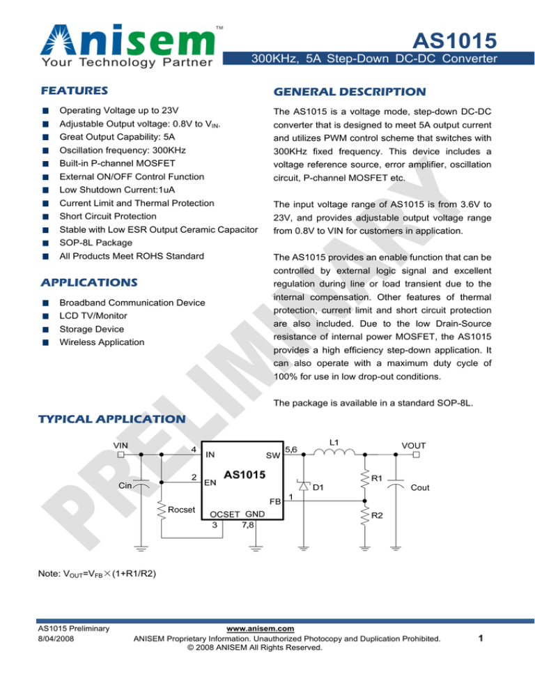
TYPICAL APPLICATION
Note: VOUT=VFB×(1+R1/R2)
AS1015 Preliminary
8/04/2008
www.anisem.com
ANISEM Proprietary Information. Unauthorized Photocopy and Duplication Prohibited.
© 2008 ANISEM All Rights Reserved.
1
AS1015
300KHz, 5A Step-Down DC-DC Converter
ABSOLUTE MAXIMUM RATINGS
PACKAGE/ORDER INFORMATION
(Note1)
TOP VIEW
Input Voltage …………………………………… +25V
SW Pin Voltage….…………………-0.5V to VIN+0.5V
FB Pin Voltage…………………………...-0.3V to VIN
EN Pin Voltage……………………-0.3V to VIN+0.3V
PD Power Dissipation (TA=25℃)…… Internal Limited
Junction Temperature ..………………………..150℃
Storage Temperature Range ………. -65℃ to 150℃
Lead Temperature(Soldering, 10sec.) …….…300℃
Note 1: Absolute Maximum Ratings are those values beyond
which the life of a device may be impaired.
PART NUMBER
PACKAGE
MARKING
AS1015KBT
SOP-8L
AS1015
ELECTRICAL CHARACTERISTICS
VCC =12V, VOUT =3.3V,TA = 25°C, unless otherwise noted.
PARAMETER
CONDITIONS
MIN
TYP
MAX
UNITS
Input Voltage Range
3.6
-
23
V
Junction Temperature Range
-40
-
125
℃
0.784
0.8
0.816
V
Feedback Voltage
ILOAD=0.1A
Oscillation Frequency
VIN =3.6~23V, ILOAD=0.2~5A
240
300
360
KHz
SCP Frequency
VIN =3.6~23V
30
50
70
KHz
Duty Cycle
VFB =0V force driver on
-
100
-
%
VIN=5V, VFB =0V
-
35
45
28
35
Internal MOSFET RDS(ON)
VIN=12V, VFB =0V
mΩ
Quiescent Current
VIN =3.6~23V, VFB =1.5V force driver off
-
3
10
mA
Shutdown Current
VEN=GND
-
1
10
uA
0.8
1.3
2.0
V
-
1
20
uA
EN Threshold Voltage
EN Pin Bias Voltage
FB Pin Bias Voltage
ILOAD=0.2A
-
0.1
0.5
uA
OCSET Pin Bias Voltage
ILOAD=0.2A
75
95
105
uA
Line Regulation
VIN =3.6~23V, ILOAD=0.2A
-
2
-
%
Load Regulation
ILOAD=0.2A~5A
-
0.1
-
%
Over Temperature Shutdown
-
150
-
Over Temperature Hysteresis
-
25
-
VIN=12V, VOUT=5V, IO=5A
-
90
-
VIN=5V, VOUT=3.3V, IO=5A
-
88
-
Thermal Resistance θJC
-
-
20
Thermal Resistance θJA
-
-
60
Efficiency: η
AS1015 Preliminary
8/04/2008
www.anisem.com
ANISEM Proprietary Information. Unauthorized Photocopy and Duplication Prohibited.
© 2008 ANISEM All Rights Reserved.
℃
%
℃/W
2
AS1015
300KHz, 5A Step-Down DC-DC Converter
PIN FUNCTIONS
PIN NUMBER
PIN NAME
1
FB
FUNCTION
This pin senses the feedback voltage to regulate the output voltage. Connect
this pin to a resistor divider to set the output voltage.
This pin allows an external logic control signal to turn on/off this device. Float
2
this pin or drive it to low level to turn-off this device, drive it to high level to
EN
turn on this device. If this feature is not needed, connect this pin to IN pin
directly.
3
OCSET
Add an external resistor from this pin to IN pin to set peak current.
The input pin of the step-down converter.
4
A suitably large capacitor must be connected from this pin to ground to
IN
bypass noise on the input of the IC.
The output pin of the step-down converter.
5, 6
SW
This pin is the switching node that supplies power to the output. Connect a
LC filter from this pin to the output load and a rectifier diode to the ground
7, 8
GND
The ground pin of the step-down converter.
Connect this pin to the circuit ground.
BLOCK DIAGRAM
AS1015 Preliminary
8/04/2008
www.anisem.com
ANISEM Proprietary Information. Unauthorized Photocopy and Duplication Prohibited.
© 2008 ANISEM All Rights Reserved.
3
AS1015
300KHz, 5A Step-Down DC-DC Converter
TYPICAL PERFORMANCE CHARACTERISTICS
VCC =12V, VOUT =3.3V,TA = 25°C, unless otherwise noted.
AS1015 Preliminary
8/04/2008
www.anisem.com
ANISEM Proprietary Information. Unauthorized Photocopy and Duplication Prohibited.
© 2008 ANISEM All Rights Reserved.
4
AS1015
300KHz, 5A Step-Down DC-DC Converter
TYPICAL PERFORMANCE CHARACTERISTICS
VCC =12V, VOUT =3.3V,TA = 25°C, unless otherwise noted.
AS1015 Preliminary
8/04/2008
www.anisem.com
ANISEM Proprietary Information. Unauthorized Photocopy and Duplication Prohibited.
© 2008 ANISEM All Rights Reserved.
5
AS1015
300KHz, 5A Step-Down DC-DC Converter
TYPICAL PERFORMANCE CHARACTERISTICS
VCC =12V, VOUT =3.3V,TA = 25°C, unless otherwise noted.
AS1015 Preliminary
8/04/2008
www.anisem.com
ANISEM Proprietary Information. Unauthorized Photocopy and Duplication Prohibited.
© 2008 ANISEM All Rights Reserved.
6
AS1015
300KHz, 5A Step-Down DC-DC Converter
APPLICATION INFORMATION
OUTPUT VOLTAGE PROGRAMMING
The device develops a band-gap between the
feedback pin and ground pin. Therefore, the output
voltage can be formed by R1 and R2. Use 1% metal
film resistors for the lowest temperature coefficient
and the best stability. Select lower resistor value to
minimize noise pickup in the sensitive feeback pin,
Keeping the device off. Once the capacitor voltage
rises above the EN pin threshold voltage, the
device will start to operate.
For example, setting at VIN=12V, RDELAY=100K,
CDELAY=0.1uF. The start-up delay time can be
calculated as below:
Vc
or higher resistor value to improve efficiency.
The output voltage is given by the following formula:
Vout
Vfb
1
R1
; where Vfb
R2
0.8V
SHORT CIRCUIT PROTECTION
This device includes short circuit protection. When
the output is shorted to ground, the protection circuit
will be triggered and force the oscillation frequency
down to approximately 50KHz. The oscillation
frequency will return to the normal value once the
output voltage or the feedback voltage rises above
0V.
Vin
1
e
T/
Ven
T>1.147ms
Where
Vc is capacitor voltage
Ven is 1.3V typical, EN pin threshold voltage
T is delay time
τ is Rdelay * Cdelay
This feature is useful in situations where the input
power source is limited in the amount of current it
can deliver. It allows the input voltage to rise to a
higher voltage before the device starts operating.
THERMAL CONSIDERATION
Thermal protection limits total power dissipation in
PEAK CURRENT SETTING
This device reserves OCSET pin to set the switching
peak current. In general, the peak current must be
1.5 times of the continuous output current. It can be
calculated as below:
Ipk
Iocset
Rocset /Rds on
Where:
this device. When the junction temperature
reaches approximately 150°C, the thermal sensor
signals the shutdown logic turning off this device.
The thermal sensor will turn this device on again
after the IC’s junction temperature cools by 25°C.
For continuous operation, do not exceed the
maximum operation junction temperature 125°C.
Ipk - Peak current
Iocset – OCSET Pin Bias Current
Rds(on) – Internal MOSFET ON-Resistance
DELAY START-UP
Uses the EN pin to provide a time delay between the
input voltage is applied and the output voltage
comes up. As the instant of the input voltage rises,
the charging of capacitor CDELAY pulls the EN pin low,
AS1015 Preliminary
8/04/2008
www.anisem.com
ANISEM Proprietary Information. Unauthorized Photocopy and Duplication Prohibited.
© 2008 ANISEM All Rights Reserved.
7
AS1015
300KHz, 5A Step-Down DC-DC Converter
PACKAGE DESCRIPTION Units: mm
Package
8-Lead Plastic SOP-8L
AS1015 Preliminary
8/04/2008
www.anisem.com
ANISEM Proprietary Information. Unauthorized Photocopy and Duplication Prohibited.
© 2008 ANISEM All Rights Reserved.
8
AS1015
300KHz, 5A Step-Down DC-DC Converter
© ANISEM Semiconductor Co., Ltd
ANISEM assume responsibility for use of any circuitry other than circuitry entirely embodied in an ANISEM product. No circuit patent licenses,
copyrights, mask work rights, or other intellectual property rights are implied. ANISEM reserves the right to make changes to their products or
specifications or to discontinue any product or service without notice. Customers are advised to obtain the latest version of relevant information to
verify, before placing orders, that information being relied on is current and complete. All products are sold subject to the terms and conditions of
sale supplied at the time of order acknowledgement, including those pertaining to warranty, patent infringement, and limitation of liability.
ANISEM warrants performance of its semiconductor products to the specifications applicable at the time of sale in accordance with ANISEM’s
standard warranty. Testing and other quality control techniques are utilized to the extent ANISEM deems necessary to support this warranty.
Specific testing of all parameters of each device is not necessarily performed.
AS1015 Preliminary
8/04/2008
www.anisem.com
ANISEM Proprietary Information. Unauthorized Photocopy and Duplication Prohibited.
© 2008 ANISEM All Rights Reserved.
9


