MP3360
Highly Integrated Photo Flash Charger
and IGBT Driver
The Future of Analog IC Technology
DESCRIPTION
FEATURES
The MP3360 is a fast, highly efficient and
precision high voltage photo-flash charger for
camera phone xenon flash.
•
•
The MP3360 has programmable peak currents
of
1.5A/1.4A/1.3A/1.2A/1.1A/1.0A/0.9A/0.8A
/0.75A/0.7A/0.65A/0.6A/0.55A/0.5A/0.45A/0.4A.
A 60V, 0.5Ω internal power switch lowers
transformer turns ratio and switching losses
associated with the primary leakage inductance
and winding capacitance. Integrated secondary
feedback resistors provide +/-2.5% output
voltage charge accuracy. MP3360 also has an
integrated IGBT driver with a regulated 2.7V
gate voltage.
•
•
•
Integrated 60V, 0.5Ω Power Switch
Single wire digital interface for current limit
programming.
2.5% Charge Accuracy
<1uA Shutdown Current
Integrated IGBT Driver with Regulated Gate
Voltage
APPLICATIONS
•
•
•
•
Mobile Phones with Xeon Flash
Digital Still Cameras
Optical Film Cameras
PDAs with Xeon Flash
“MPS” and “The Future of Analog IC Technology” are Registered Trademarks of
Monolithic Power Systems, Inc.
MP3360 is available in the 10-pin, 2X2 flip chip
package.
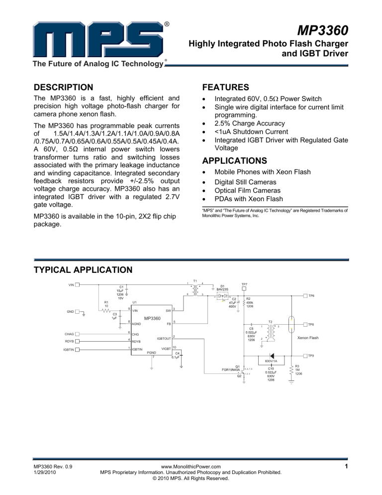
TYPICAL APPLICATION
1
VIN
4
TP7
3
GND
U1
9
8
CHAG
RDYB
IGBTIN
6
4
1
VIN
SW
MP3360
FB
AGND
CHG
IGBTOUT
RDYB
IGBTIN
VIGBT
TP6
R2
499k
1206
3
R1
10
2
1
6
T1
3
T2
5
1
2
TP8
3
Xenon Flash
2
10
PGND
7
TP9
600V/1A
5, 6, 7, 8
4
MP3360 Rev. 0.9
1/29/2010
1, 2, 3
www.MonolithicPower.com
MPS Proprietary Information. Unauthorized Photocopy and Duplication Prohibited.
© 2010 MPS. All Rights Reserved.
R3
1M
1206
1
MP3360 – HIGHLY INTEGRATED PHOTO FLASH CHARGER AND IGBT DRIVER
ORDERING INFORMATION
Part Number*
Package
Top Marking
Free Air Temperature (TA)
MP3360
10-pin, 2x2 Flip QFN
4KY
-40°C to +85°C
For Tape & Reel, add suffix –Z (e.g. MP3360DG–Z);
For RoHS Compliant Packaging, add suffix –LF(e.g. MP3360DG–LF–Z)
PACKAGE REFERENCE
TOP VIEW
VIGBT
10
IGBTIN
1
9
VIN
IGBTOUT
2
8
AGND
SW
3
7
PGND
RDYB
4
6
CHG
5
FB
ABSOLUTE MAXIMUM RATINGS (1)
Recommended Operating Conditions
VIN to GND .........................................-0.3Vto 6V
CHG, IGBTIN, IGBTOUT, VIGBT,
RDYB to AGND .................................-0.3Vto 6V
FB to AGND ...................................-60V to 350V
SW to AGND...................................-0.3V to 60V
PGND to AGND ...........................-0.3V to +0.3V
2X2, 10 pin Flip Chip Thermal Resistance
Operating Temperature Ranges .........................
............................................. -20°C to +85°C
Storage Temperature............... -55°C to +150°C
Junction Temperature ............................ +150°C
(2)
Continuous Power Dissipation (TA = +25°C)
………………………………………………....1.6W
Lead Temperature (Solder).....................+260°C
Supply Voltage VIN .............................2.5V to 6V
Operating Junct. Temp (TJ)...... -40°C to +125°C
Thermal Resistance
(4)
θJA
(3)
θJC
2x2 Flip Chip ...........................80 ...... 16 ... °C/W
Notes:
1) Exceeding these ratings may damage the device.
2) The maximum allowable power dissipation is a function of the
maximum junction temperature TJ (MAX), the junction-toambient thermal resistance θJA, and the ambient temperature
TA. The maximum allowable continuous power dissipation at
any ambient temperature is calculated by PD (MAX) = (TJ
(MAX)-TA)/θJA. Exceeding the maximum allowable power
dissipation will cause excessive die temperature, and the
regulator will go into thermal shutdown. Internal thermal
shutdown circuitry protects the device from permanent
damage.
3)
The device is not guaranteed to function outside of its operating
conditions.
4) Measured on JESD51-7, 4-layer PCB.
MP3360 Rev. 0.9
1/29/2010
www.MonolithicPower.com
MPS Proprietary Information. Unauthorized Photocopy and Duplication Prohibited.
© 2010 MPS. All Rights Reserved.
2
MP3360 – HIGHLY INTEGRATED PHOTO FLASH CHARGER AND IGBT DRIVER
ELECTRICAL CHARACTERISTICS
VIN = V (CHG) = 3.6V, TA = +25°C, unless otherwise noted.
Parameter
Photoflash Capacitor Charger
VIN Voltage Range
VIN UVLO
VIN Quiescent Current
VIN Quiescent Current
Shutdown Current from VIN
VSW Leakage Current
SW ON Resistance between SW
and GND
Pull-down Resistance of CHG pin
IPEAK1
IPEAK2
Charge completion detect voltage
at FB
FB Resistance
DCM Comparator threshold
RDYB Leakage Current
RDYB Output Low Voltage
MAX TON
Thermal Shutdown
Charge Input High Voltage
Charge Input Low Voltage
tHI
tLO
tEN_delay
tPW
MP3360 Rev. 0.9
1/29/2010
Conditions
Min
Typ
2.5
Rising edge, hysteresis = 200mV
typical
V(CHG)=High, V(SW) = 0
V(CHG)=High, V(FB) = 325V
V(CHG)=Low, VIN =3.6V
VIN=3.6V, VSW=60V, in Shutdown
1
Switch turn-on
V(CHG)=3.6V
Program for Highest Current Limit
Program for Lowest Current Limit
Max
Unit
6
V
2.5
V
2
150
1
1
mA
µA
µA
µA
Ω
0.5
1.3
100
1.5
0.4
1.7
0.6
kΩ
A
A
290
298
308
V
V(FB)=30V
303
5
V(RDYB)=3.6V
ISINK= 2mA
Maximum TON time
Rising edge, hysteresis = 15°C
0.1
0.2
70
150
120
2.4
0.6
0.1
0.1
30
Vin=2.7V-5.5V
www.MonolithicPower.com
MPS Proprietary Information. Unauthorized Photocopy and Duplication Prohibited.
© 2010 MPS. All Rights Reserved.
60
kΩ
V
µA
V
µS
°C
V
V
µS
µS
µS
µS
3
MP3360 – HIGHLY INTEGRATED PHOTO FLASH CHARGER AND IGBT DRIVER
PIN FUNCTIONS
Pin
1
2
3
4
5
Name
IGBTIN
IGBTOUT
SW
RDYB
FB
6
CHG
7
8
PGND
AGND
9
VIN
10
VIGBT
MP3360 Rev. 0.9
1/29/2010
Function
Logic Input Pin for IGBT Drive.
Output Drive for IGBT Gate. Connect this pin to the gate of the IGBT.
Switch Pin. This is the drain of the internal power switch.
Open-Drain Power-Ready Output. RDYB becomes low when the output voltage is reached.
Feedback Pin. Its trip voltage is 298V
Charge Enable Pin. A low to high transition on this pin puts the part into power delivery
mode. Once the target voltage is reached, the part will stop charging the output. Toggle
this pin will start charging again. Bring this pin low will terminate the power delivery and put
the part in shutdown. This pin can be also used to program the peak current regulation. See
the description for current programming.
Power Ground
Analog ground. Tie it directly to local ground plane.
Input Supply Pin. Connect it to system supply voltage. Bypass VIN to GND with a 0.1uF or
greater ceramic capacitor.
2.7V LDO output. VIGBT is the supply voltage for IGBT gate driver. Bypass VIGBT with
0.1uF cap to GND.
www.MonolithicPower.com
MPS Proprietary Information. Unauthorized Photocopy and Duplication Prohibited.
© 2010 MPS. All Rights Reserved.
4
MP3360 – HIGHLY INTEGRATED PHOTO FLASH CHARGER AND IGBT DRIVER
TYPICAL PERFORMANCE CURVES
Line Regulation
Efficiency vs VOUT
3900
3600
ISET=1.5V
3300
COUT=100uF
3000
VOUT=300V
2700
2400
2100
1800
1500
1200 ISET=1.5V
900 COUT=47uF
VOUT=300V
600
2.5 3 3.5 4 4.5 5 5.5 6 6.5
INPUT VOLTAGE (V)
80
VIN=6V
77
74
VIN=4.5V
71
68
VIN=3V
65
62
59
56
53
50
70
110 150 190 230 270 310
VOUT (V)
NORMALIZED OUTPUT VOLTAGE (V)
ISET=1.5A
EFFICIENCY ( % )
CHARGE TIME (mS)
Charge Time vs.
Input Voltage
1.001
1
0.999
0.998
ISET=1.5V
COUT=47uF
VOUT=300V
0.997
0.996
0.995
2.5
3 3.5 4 4.5 5 5.5
INPUT VOLTAGE (V)
Switching Waveform
Switching Waveform
Charging Waveform
VIN = 3.3V, VOUT = 300V,
ISET = 1.5A, COUT = 47uF
VIN = 5.0V, VOUT = 300V,
ISET = 1.5A, COUT = 47uF
VIN = 3.3V, VOUT = 300V,
ISET = 1.5A, COUT = 47uF
6 6.5
VCHG
2V/div.
VSW
20V/div.
VOUT
100V/div.
VSW
20V/div.
VOUT
100V/div.
ISW
1A/div.
ISW
1A/div.
2us/div.
VRDYB
2V/div.
VOUT
100V/div.
ISW
500mA/div.
2us/div.
400µ s/div.
Charging Waveform
Charging Waveform
Charging Waveform
VIN = 5.0V, VOUT = 300V,
ISET = 1.5A, COUT = 47uF
VIN = 3.3V, VOUT = 300V,
ISET = 1.5A, COUT = 100uF
VIN = 5.0V, VOUT = 300V,
ISET = 1.5A, COUT = 100uF
VCHG
2V/div.
VRDYB
2V/div.
VOUT
100V/div.
VCHG
2V/div.
VRDYB
2V/div.
VOUT
100V/div.
VCHG
2V/div.
VRDYB
2V/div.
VOUT
100V/div.
ISW
500mA/div.
ISW
500mA/div.
ISW
500mA/div.
200µ s/div.
MP3360 Rev. 0.9
1/29/2010
1s/div.
www.MonolithicPower.com
MPS Proprietary Information. Unauthorized Photocopy and Duplication Prohibited.
© 2010 MPS. All Rights Reserved.
400µ s/div.
5
MP3360 – HIGHLY INTEGRATED PHOTO FLASH CHARGER AND IGBT DRIVER
BLOCK DIAGRAM
Figure 1—Functional Block Diagram
MP3360 Rev. 0.9
1/29/2010
www.MonolithicPower.com
MPS Proprietary Information. Unauthorized Photocopy and Duplication Prohibited.
© 2010 MPS. All Rights Reserved.
6
MP3360 – HIGHLY INTEGRATED PHOTO FLASH CHARGER AND IGBT DRIVER
OPERATION
The MP3360 controlled flyback charger
operates in critical conduction mode with peak
current set by the CHG pin. The output voltage
is divided down through internal 300: 1 resistive
divider from the positive terminal of the
transformer secondary (FB pin) and compares it
with the internal 1.2V reference. The low to
high transition of the CHG pin will enable the
flyback converter to switch.
A constant TOFF of 20µs is used when the
output voltage is below 20V to avoid inrush
current. The boundary mode operation will
follow to minimize charge time when the output
voltage is above 20V. A minimum TOFF of 200ns
serves as blanking for turn off transition. The
circuit will stop switching and RDYB will be
pulled low once the flash capacitor is charged
to 300V, a value set by the internal 300:1 R
divider and 1.2V reference. VIGBT will be
regulated to 2.7V.
When the charge is full,
then part will shut down its internal circuitry with
less than 1uA drawn from VIN. Toggling the
CHG pin will restart charge cycle. Bringing the
CHG pin low terminates the power delivery and
put the part in shutdown. A maximum TON timer
prevents pulling current from a depleted battery.
If the ON time exceeds maximum TON, the
switch is forced OFF regardless of the IPEAK
detection.
First Two required to initiate
tHI tLO
programming
CURRENT LIMIT PROGRAMMING
The current limit can be programmed using the
CHG pin. After asserting the CHG, it should be
held high for at least 30us. After that, it takes
two pulses to enter the programming mode. In
the programming mode, each pulse advances
the internal counter to the next higher current
limit by 50mA until 750mA is reached and by
100mA increments beyond 750mA. The first
pulse is for 400mA current limit. The next pulse
will set the current limit to 450mA, etc. This
programming should be done within 60us.
Otherwise, the programming pulses will be
ignored after the programming window expires.
When you have advanced to the desired
current limit setting, the high state should be
held to make the part switch with the set current
limit. To set the current limit to 1.5A (highest
possible), the previous procedure is not
necessary. Asserting and holding high the CHG
pin will make the part switches with a 1.5A
current limit. See the following timing diagram
for detailed timing information.
Falling edge of the following
pulses advance the internal
counter
CHG
tEN-delay
400mA
600mA
ON
(Internal)
ENPRG
(Internal)
tPW
During this time, the low state of CHG can not
shut-down the part.
Switching starts.
ILIM Programming Timing Diagram
(600mA Current Limit)
MP3360 Rev. 0.9
1/29/2010
www.MonolithicPower.com
MPS Proprietary Information. Unauthorized Photocopy and Duplication Prohibited.
© 2010 MPS. All Rights Reserved.
7
MP3360 – HIGHLY INTEGRATED PHOTO FLASH CHARGER AND IGBT DRIVER
PACKAGE INFORMATION
QFN10 (2mm x 2mm)
NOTICE: The information in this document is subject to change without notice. Users should warrant and guarantee that third
party Intellectual Property rights are not infringed upon when integrating MPS products into any application. MPS will not
assume any legal responsibility for any said applications.
MP3360 Rev. 0.9
1/29/2010
www.MonolithicPower.com
MPS Proprietary Information. Unauthorized Photocopy and Duplication Prohibited.
© 2010 MPS. All Rights Reserved.
8
