Low-Power HCSL vs. Traditional HCSL
AN-879
APPLICATION NOTE
Introduction
Low-Power HCSL (LP-HCSL) was developed to lower the power consumption of traditional HCSL drivers. Other major
advantages of LP-HCSL were soon discovered, including better performance driving long traces, easy AC-coupling, reduced
board area, easier board routing and Bill of Material (BOM) reduction. These advantages will be discussed in this application
note. It is important to note that an HCSL receiver cannot tell the difference between a traditional HCSL driver and a LP-HCSL
driver.
IDT has been awarded patents US 7342420 B2, US 7821297 B2 and US 7830177 B2 for this technology.
Functionality
Traditional HCSL outputs steer a constant 15mA current between true and complement outputs of a differential pair. This results
in a continuous power consumption of ~50mW from 3.3V for each differential HCSL output pair.
Low Power HCSL uses a push-pull voltage drive as opposed to current drive with traditional HCSL. This results in a current
consumption of approximately 4 to 5mA. Supply current flows in the driver only during the time a rising edge is traveling from the
driver to the end target and then back to the driver (round trip flight time).
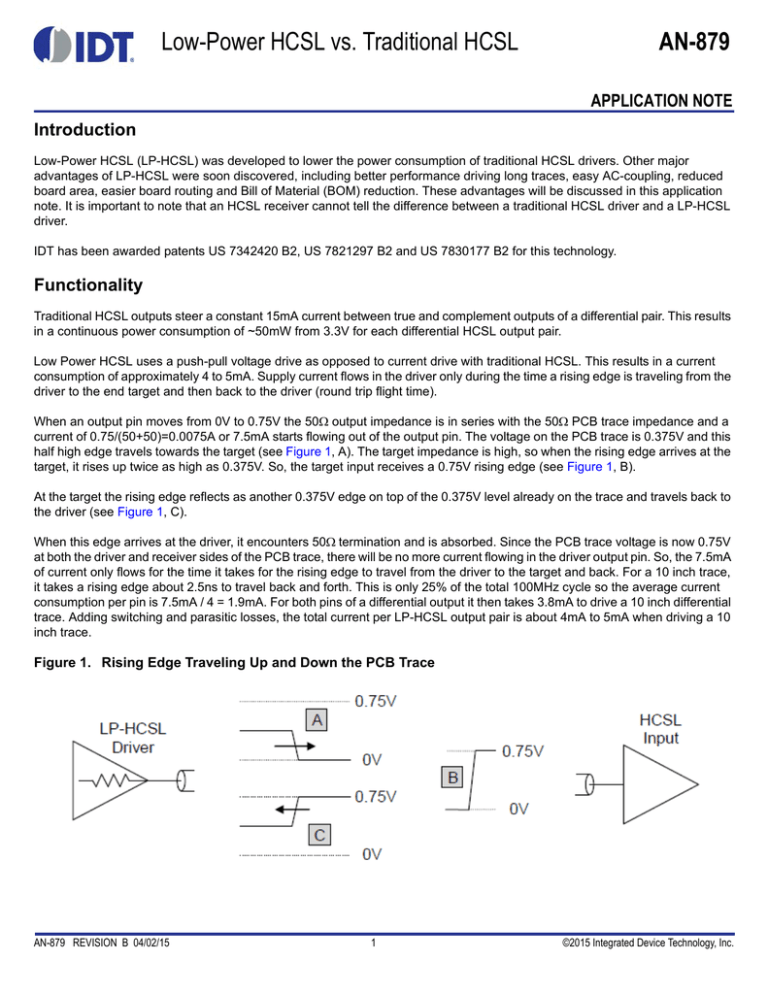
When an output pin moves from 0V to 0.75V the 50 output impedance is in series with the 50 PCB trace impedance and a
current of 0.75/(50+50)=0.0075A or 7.5mA starts flowing out of the output pin. The voltage on the PCB trace is 0.375V and this
half high edge travels towards the target (see Figure 1, A). The target impedance is high, so when the rising edge arrives at the
target, it rises up twice as high as 0.375V. So, the target input receives a 0.75V rising edge (see Figure 1, B).
At the target the rising edge reflects as another 0.375V edge on top of the 0.375V level already on the trace and travels back to
the driver (see Figure 1, C).
When this edge arrives at the driver, it encounters 50termination and is absorbed. Since the PCB trace voltage is now 0.75V
at both the driver and receiver sides of the PCB trace, there will be no more current flowing in the driver output pin. So, the 7.5mA
of current only flows for the time it takes for the rising edge to travel from the driver to the target and back. For a 10 inch trace,
it takes a rising edge about 2.5ns to travel back and forth. This is only 25% of the total 100MHz cycle so the average current
consumption per pin is 7.5mA / 4 = 1.9mA. For both pins of a differential output it then takes 3.8mA to drive a 10 inch differential
trace. Adding switching and parasitic losses, the total current per LP-HCSL output pair is about 4mA to 5mA when driving a 10
inch trace.
Figure 1. Rising Edge Traveling Up and Down the PCB Trace
AN-879 REVISION B 04/02/15
1
©2015 Integrated Device Technology, Inc.
AN-879
HCSL Driver Topology
Figure 2. Comparing Traditional and Low-Power HCSL Driver Topology
Traditional HCSL
Current Driver
Low Power HCSL
Push-Pull Driver
RS
RS
RT
Advantages of LP-HCSL
1) 3x to 9x Lower Power Consumption
We have already seen that the LP-HCSL driver uses 1/3 the current of the traditional HCSL driver (5mA versus 15mA).
From Figure 2, we see that the 15mA current source is supplied by the VDD rail of the traditional HCSL device. Practical
considerations limit the lower limit of this power rail to 2.5V. The LDO used in the LP-HCSL driver can be powered from
any voltage from VDD down to the output voltage + LDO headroom (or 800mV + 250mV = 1.05V). If the traditional HCSL
output power supply is 3.3V and the LP-HCSL power supply is 1.05V, we see a 3x reduction in power supply voltage.
With 1/3 the current and 1/3 the voltage rail, LP-HCSL can achieve a 9x reduction in power.
LP-HCSL outputs also allow the output amplitude to be adjusted (up or down) by adjusting the LDO setting. Many IDT
LP-HCSL devices allow amplitude adjustment via SMBus registers.
2) Better Drive of Long Traces
PCIe clocks are specified to have slew rates of 0.6V/ns to 4.0V/ns. LP-HCSL outputs provide higher slew rates when
driving long traces. A traditional HCSL driver depends upon the external 50 termination to make the falling edge of the
clock. This makes rise/fall matching more difficult, since only the rising edge of the clock is under control of the traditional
HCSL output. The LP-HCSL output controls both the rising and falling edge of the clock. The faster slew rates of
LP-HCSL are especially important when driving long PCB traces and/or passing through connectors to other PCBs in
the system. Faster slew rates at the start of a long trace will result in faster slew rates at the end of long traces. Faster
slew rates at a receiver translate into lower jitter and lower bit error rates.
IDT used a Nelco test board to compare the slew rate of traditional HCSL and LP-HCSL after driving 30-inch traces.
From Figure 3, we see that LP-HCSL was observed to be almost 50% faster than traditional HCSL at the end of a 30
inch long trace.
LOW-POWER HCSL VS. TRADITIONAL HCSL
2
REVISION B 04/02/15
AN-879
Figure 3. After Passing Through 30 inch Long PCB Trace
Traditional HCSL
LP-HCSL
+0.84V/ns Rise and -0.88V/ns Fall
+01.24V/ns Rise and -1.18V/ns Fall
Yellow and Green are the true and complementary outputs on the differential output pair.
The slew rates are measured in +/-75mV window around the crossing point.
3) Easy AC-Coupling
LP-HCSL does not require a DC coupled termination like traditional HCSL does. You can add capacitors in series with
LP-HCSL signals without affecting the signal swing or termination properties. With traditional HCSL care has to be taken
that a DC path to ground remains when adding AC coupling and this may require extra components.
4) Smaller Board Area, Easier Board Routing and Reduced Bill of Materials
LP-HCSL outputs do not need the termination resistor to ground. This saves 2 of the 4 termination resistors required by
a standard HCSL differential output. IDT also integrates the series termination in some of its LP-HCSL drivers,
eliminating all 4 termination resistors, so all that is required is a PCB trace between the driver output and the target input.
Power dissipation in the termination resistors prevents their integration in traditional HCSL drivers, especially with a
large amount of outputs on one die.
Figure 4. Board Area Savings with LP-HCSL
2.3x smaller
Traditional HCSL termination uses a 50 resistor to ground at the end of the PCB trace. Later, another method was
introduced, placing the 50to ground near the driver. This is called “Source Termination” and allows for the clock to
pass through connectors that can be unplugged while the circuit is active (hot swapping). LP-HCSL has its termination
at the driver side by definition, and it can work with end terminations. This setup is referred to as double termination
(more on this in a moment). Source termination versus end termination makes no difference to the receiver.
REVISION B 04/02/15
3
LOW-POWER HCSL VS. TRADITIONAL HCSL
AN-879
Figure 5. Traditional HCSL Termination
The series resistors RS are needed to avoid excessive ringing.
End
Termination
Source
Termination
Figure 6. LP-HCSL Termination
The termination resistors (RS) are now in series with the clock line, near the driver. The driver itself is designed to have 17
output impedance so it requires another 33to match 50PCB traces. The schematic on the right has the termination resistors
integrated so no external components are needed to drive 50PCB traces.
Traditional HCSL doesn't use the driver itself as part of the termination. Besides the 50 termination resistor, traditional HCSL
needs an additional 33series resistor to avoid a reflection and ringing between the driver and the 50 terminated trace. The
LP-HCSL concept combines the main termination and ringing avoidance in the same 33 series resistor, reducing the parts
count.
Certain applications use 85differential traces (or 42.5single ended). For these applications, we recommend RS=27 IDT
also offers clocks with the 27RS integrated for 85systems.
Double Termination: Certain receivers may have a 100differential termination resistor in the chip. These receivers are usually
more generic, can handle a wide range of amplitudes and common-mode voltages, and may require AC coupling of the clock
signals. LP-HCSL drivers can readily drive double terminations. Having termination resistors at both the source and receiver
lowers the amplitude to about 400mVpp at each pin (800mVpp differential). Usually it is not a problem for this type receiver to
work with the smaller amplitudes. The 400mVpp (800mVpp differential) level even exceeds the 150mVpp (300mVpp differential)
input swing spec for PCIe reference clocks.
Conclusion
Low Power HCSL not only reduces power significantly, it also better drives long traces, saves board area, reduces BOM costs,
and more easily drives AC-coupled transmission lines. This makes Low Power HCSL the choice for future designs.
Table 1: Traditional HCSL versus Low Power HCSL Overview
Traditional HCSL
LP-HCSL
Power Supply Current per driver
15mA
4 ~ 5mA
Available output driver VDD voltages
Down to 2.5V
Down to 1.05V
Slew Rate after 30" PCB trace
0.8V/ns
1.2V/ns
Passives required per differential output
4 resistors
None for integrated termination
LOW-POWER HCSL VS. TRADITIONAL HCSL
4
REVISION B 04/02/15
Corporate Headquarters
Sales
Tech Support
6024 Silver Creek Valley Road
San Jose, CA 95138 USA
1-800-345-7015 or 408-284-8200
Fax: 408-284-2775
www.IDT.com
email: clocks@idt.com.
DISCLAIMER Integrated Device Technology, Inc. (IDT) and its subsidiaries reserve the right to modify the products and/or specifications described herein at any time and at IDT’s sole discretion. All information in
this document, including descriptions of product features and performance, is subject to change without notice. Performance specifications and the operating parameters of the described products are determined
in the independent state and are not guaranteed to perform the same way when installed in customer products. The information contained herein is provided without representation or warranty of any kind, whether
express or implied, including, but not limited to, the suitability of IDT’s products for any particular purpose, an implied warranty of merchantability, or non-infringement of the intellectual property rights of others. This
document is presented only as a guide and does not convey any license under intellectual property rights of IDT or any third parties.
IDT’s products are not intended for use in applications involving extreme environmental conditions or in life support systems or similar devices where the failure or malfunction of an IDT product can be reasonably
expected to significantly affect the health or safety of users. Anyone using an IDT product in such a manner does so at their own risk, absent an express, written agreement by IDT.
Integrated Device Technology, IDT and the IDT logo are registered trademarks of IDT. Product specification subject to change without notice. Other trademarks and service marks used herein, including protected
names, logos and designs, are the property of IDT or their respective third party owners.
Copyright ©2015 Integrated Device Technology, Inc.. All rights reserved.


