AVR354: Using the Deep Under-Voltage
Recovery Mode (DUVR)
8-bit
Microcontrollers
Features
• Charging Li-Ion battery cells from 0V without using a pre-charge FET or current
limiting resistor.
• Current limited charger kept in pre-charge mode by regulating the voltage at the
positive battery terminal below fast-charge threshold.
• MCU fully operational throughout the charging sequence.
Application Note
1 Introduction
Charging Li-ion battery cells from a deeply discharged condition and at the same
time keep full control of the charging sequence, is a challenge in many
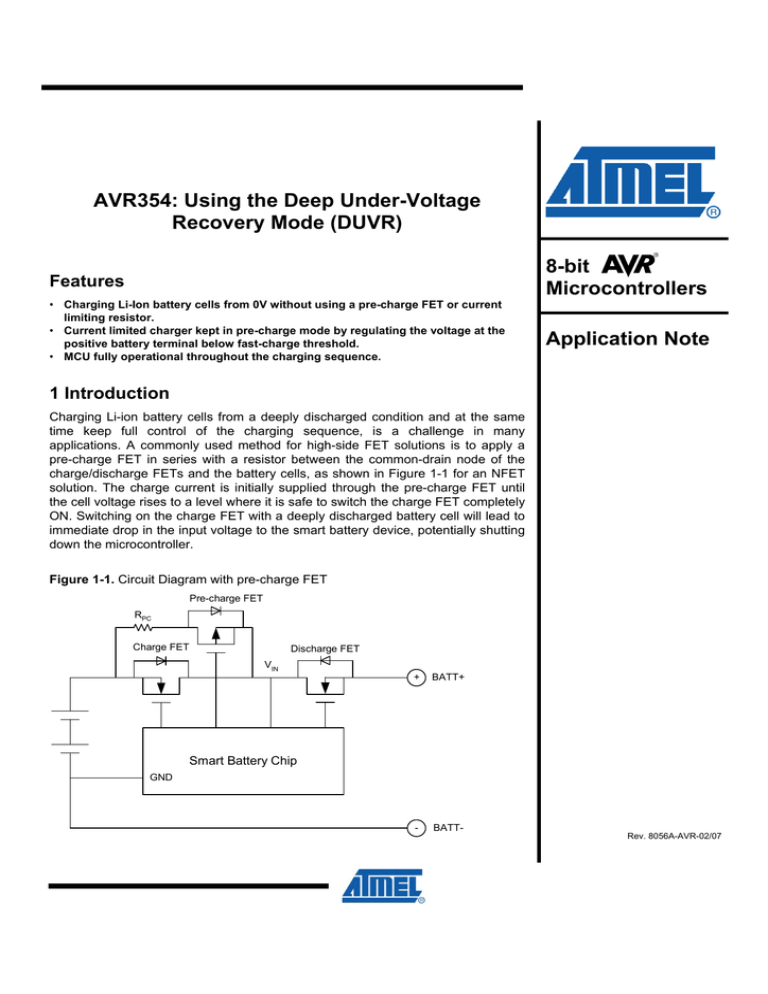
applications. A commonly used method for high-side FET solutions is to apply a
pre-charge FET in series with a resistor between the common-drain node of the
charge/discharge FETs and the battery cells, as shown in Figure 1-1 for an NFET
solution. The charge current is initially supplied through the pre-charge FET until
the cell voltage rises to a level where it is safe to switch the charge FET completely
ON. Switching on the charge FET with a deeply discharged battery cell will lead to
immediate drop in the input voltage to the smart battery device, potentially shutting
down the microcontroller.
Figure 1-1. Circuit Diagram with pre-charge FET
Pre-charge FET
RPC
Charge FET
Discharge FET
VIN
+
BATT+
-
BATT-
Smart Battery Chip
GND
Rev. 8056A-AVR-02/07
An obvious disadvantage of the scheme presented above, is the extra system cost of
the external pre-charge FET and series resistor, and the excessive power dissipated
in the external resistor.
2 Charger with current limitation
Many Li-ion battery chargers have a built-in current limitation for pre-charging of
deeply discharged cells. The current supplied by the charger is determined by the
voltage seen at the positive battery pack terminal, VBATT. If the voltage on the BATT
terminal is below a pre-defined (or programmable) fast-charge threshold VFC, the
charger will supply a pre-charge current IPC. Above the fast-charge threshold the
charger will source a fast-charge current, IFC. A typical I-V characteristic for a charger
with current limitation is shown in Figure 2-1. The actual value of VFC must be
confirmed for the charger that is used in the application.
The charger usually has a detection time tDET from the battery is inserted in the
charger until the charge cycle begins. During this time, the charger supplies a precharge current. After tDET has expired, the charger measures the voltage on the BATT
terminal before starting the charging sequence. If VBATT is below the fast-charge
threshold when tDET expires, this indicates that the cells are deeply discharged, and
the charger starts up in the Pre-charge mode. Correspondingly, if the voltage is above
the fast-charge threshold, the charger starts up directly in Fast-charge mode.
Figure 2-1. Typical charge current as function of time for a current-limited charger.
ICHARGE
IFC
IPC
Pre - charge
Fast - charge
Voltage Regulation
t
3 Deep Under-Voltage Recovery (DUVR) mode – theory of operation
DUVR mode represents the intelligent pre-charge mode for Atmel’s smart battery
microcontrollers ATmega16HVA, ATmega8HVA, ATmega8HVD and ATmega4HVD.
It is intended for controlled charging of cells even when the cell voltage is below the
minimum operating voltage of the chip. The charging is done without using a precharge FET or current limiting resistor, and assumes that the charger is currentlimited during the pre-charge phase. ATmega16HVA is used as an example in this
application note, but unless otherwise noted one can assume that any of the devices
can be used. The operating circuit is shown in Figure 3-1.
2
AVR354
8056A-AVR-10/08
AVR354
Figure 3-1. Operating circuit.
- VDS , Charge FET +
VIN
OC
VFET
+
BATT+
-
BATT-
OD
ATmega16HVA
GND
The principle is to keep the VFET node sufficiently high to ensure stable chip
operation while keeping the positive battery terminal voltage (VBATT) below the fastcharge threshold of the charger when the cell voltage is low. In DUVR mode the
charge FET is completely controlled by autonomous hardware, overriding the
software-controlled charge FET Enable (CFE) bit. The charge FET is switched partly
ON, and provides a path for the pre-charge current. VFET is regulated at a constant
level that is above the minimum operating voltage of the smart battery chip while
keeping VBATT below the fast-charge threshold of the charger. This is done by
regulating the charge FET resistance to a point that provides a suitable voltage drop
(VDS, CFET) between VFET and the battery cell.
As the cell voltage increases, VDS, CFET will gradually decrease, and eventually the
charge FET is switched completely ON. At this point it is safe to exit DUVR mode as
long as software makes sure that the charge FET is enabled (CFE bit is set). A
complete application example is given in section 6.
As a safety precaution, the charge FET will always be switched OFF during RESET
or if a Battery Protection event has occurred (see data sheet for details on Battery
Protection). This functionality is fully autonomous and independent of the DUVR
mode operation. The requirement of disabling the charge FET during the RESET
mode is the reason why DUVR mode cannot be enabled before the start-up time of
the chip has expired. Hence, the smart battery chip provides full safety for the battery
pack even though autonomous hardware controls the charge FET in Pre-charge
mode.
4 System design considerations
Some important considerations have to be taken into account before using the Deep
Under-Voltage Recovery mode. The following subsections contain the information
needed to utilize DUVR mode in an optimized way.
4.1 Avoiding premature fast-charge
In order to keep the voltage at the BATT terminal (VBATT) lower than a specified fastcharge threshold during pre-charge, it is important to consider the parameters of the
external discharge FET. VBATT in DUVR mode for deeply discharged battery cells can
be calculated as specified in Equation 4-1.
3
8056A-AVR-10/08
Equation 4-1. Voltage at positive battery pack terminal.
VBATT = VFET DUVR + VB
VFETDUVR represents the regulated VFET voltage in DUVR mode for low cell
voltages, and VB is the voltage drop over the body-diode of the discharge FET. Note
that the VFET voltage will eventually increase above VFETDUVR when the cell voltage
exceeds VFETDUVR, so the equation is only valid as long as the cell voltage is low. If
the fast-charge threshold of the charger for an application is VFC the maximum
allowed body diode drop of the discharge FET is given in Equation 4-2.
Equation 4-2. Maximum allowable DFET body diode voltage drop.
VB, max = VFC - VFET DUVR - margin
Using VFC =3.0V and VFETDUVR =2.1V with 100mV margin, this gives a maximum
allowed voltage drop of 800mV over the diode. For pre-charge currents in the order of
100mA, this voltage will never be exceeded for most FETs used in smart battery
applications.
In case a discharge FET with high VB is used, or the fast-charge threshold of the
charger is very low, the system may switch on the discharge FET even during precharge to eliminate VB from Equation 4-1.
Opening the discharge FET while charging, may increase the need to check if the
charger is still connected. The presence of a charger can easily be measured by
monitoring the polarity of the CC-ADC conversion results (ATmega8HVA/16HVA). If a
discharge current (or no current) is flowing, this indicates that the charger has been
removed and the DFET could be disabled to reduce the risk of the battery cells being
drained unintentionally.
The battery cells will be protected from high charge and discharge currents during the
complete charging cycle as long as the Battery Protection circuitry is enabled.
4.2 Selecting correct start-up time.
It is important to harmonize the start-up time of the ATmega8HVA/16HVA, and
ATmega4HVD/8HVD with the tDET parameter of the charger. This will ensure that the
charger never enters Fast-charge mode unintentionally. The start-up time of the
microcontroller is mainly determined by the Start-Up Time (SUT) fuse settings.
However, some other parameters should also be considered in the system design.
The timing values involved in the start-up scheme are listed in Table 4-1.
Table 4-1. System level start-up considerations.
Ref
Parameter
Time(1)
Comment
1
Time from charger connected until the internal
Power-on Reset is released.
5 ms
Typical value, depending on size of external
capacitor CREG.
2
Time from Power-on Reset is released until
Internal reset is released
4-512ms
Nominal range, depending on SUT fuse settings.
Actual range depends on ULP oscillator frequency.
3
Time from Internal reset is released until DUVR
mode is enabled
0 ms
Enabled immediately after reset.
4
Time from DUVR mode enabled until VFET voltage
stabilizes at VFETDUVR
1ms
Typical value, depending on cell voltage and type
of FET.
5
Total time from charger connected to DUVR mode
is efficient
10-518 ms
Nominal value depending on SUT fuse settings,
calculated as sum of points 1 through 4.
4
AVR354
8056A-AVR-10/08
AVR354
Ref
Parameter
Time(1)
Comment
6
Time from Internal reset is released until discharge
FET can be enabled by application code
1ms
Depending on SW implementation.
7
Time from the discharge FET is enabled in
application code until VB is reduced
1ms
Typical value, depending on VFET and type of
FET.
8
Time from charger connected until VB is reduced
11-519ms
Nominal value depending on SUT fuse settings,
calculated as sum of points 1, 2, 6 and 7.
Notes:
1. Values in this column are typical values for a given application. Actual values may deviate from these numbers and
must be checked explicitly for each application. For chip parameters that have a minimum and maximum value
specified in the data sheet, worst-case considerations should be used if timing is critical.
Once the internal reset is released, DUVR mode is entered as default. For low cell
voltages, VFET will stabilize at the VFETDUVR level as soon as the charge FET has
been sufficiently switched ON by hardware. For more details on SUT fuse selection
and start-up please refer to the datasheet.
The tDET parameter is important to consider in the system design, since VBATT will rise
above the fast-charge threshold during start-up. Selecting a start-up time for the
smart battery microcontroller that is longer than tDET, may bring the charger into Fastcharge mode too soon.
4.3 Minimizing power consumption
Since DUVR mode is using a clocked regulation scheme to regulate VFET, this mode
of operation always requires a fixed, high frequency clock. In practice this means that
the Fast RC oscillator of the chip will always be enabled in DUVR mode independent
of the various sleep modes of the chip. For the Power Save sleep mode, DUVR mode
will increase the power consumption significantly. As long as the charger is
connected, the increased power consumption is insignificant. However, the
application should make sure to always disable DUVR mode whenever it is not
needed to avoid excessive current consumption during battery discharge. This is
especially important when using the deep sleep modes.
4.4 Enabling charge FET when cell voltage is too low.
If the charge FET is switched completely ON (charge FET enabled by software)
before the cell voltage has reached a level where the chip can operate, VFET drops
quickly and the Voltage Regulator can no longer keep the VREG voltage at a
sufficient level. For ATmega8/16HVA, the chip enters BOD reset when the VREG
voltage drops below the BOD level. The BOD reset immediately switches off the
charge FET, causing the VFET voltage to rise again if a charger is present. This
causes the chip to recover from BOD reset almost immediately and normal operation
can be resumed once the start-up time after reset has elapsed. For ATmega4/8HVD,
the chip enters BLOD reset/power off when VREG drops too low.
4.5 Premature charger disconnection /pulse charging
If the charger is using a pulse-charging scheme or for any reason the charger is
disconnected when the cell voltage is below the minimum operating voltage of the
chip, the device will enter power-off when either VFET or VREG drops too low. When
the charger is switched on again, a normal start-up sequence from Power-off will take
place.
5
8056A-AVR-10/08
If the charger is re-connected or the pulse-charging is resumed before VFET or
VREG drop below their minimum values, the chip will continue normal operation
without entering BOD reset or Power-off.
5 Application example
This section includes an example of a system design including start-up from power-off
using the DUVR mode and a current-limited charger. The following assumptions are
made:
• Cell voltage (VCELL) is initially 1.0V and the chip is in power-off mode.
• The fast-charge threshold of the charger is 3.0V
• The detection time of the charger, tDET = 60ms
• The body-diode drop of the discharge FET is 0.5V@50mA pre-charge current
Since the body-diode drop of the discharge FET is low compared to the fast-charge
threshold (VFC) of the charger, the discharge FET is switched off during initial
charging. The start-up time for the microcontroller is set to 32ms to ensure that the
positive battery pack terminal is regulated below VFC before the battery is detected.
The charging sequence is illustrated in Figure 5-1. The operating circuit is described
in Figure 1-1.
Figure 5-1. Application example (1-cell application).
V [V]
VB
VFC
BATT
VB
VFETDUVR
VFET
VCELL
1V
t0 < tSTART-UP > t1
t2
tDET
t3
Pre-charge
t4
t5
Fast-charge
t6
t
Voltage Regulation
ICHARGE
IFC
IPC
t
DUVRD
CFE
DFE
6
AVR354
8056A-AVR-10/08
AVR354
An explanation to the events shown in Figure 5-1 is listed in Table 5-1.
Table 5-1. Explanation to Figure 5-1.
Time
Comment
t=t0
The charger is connected. Both the charge FET and the
discharge FET are switched completely OFF, causing
VFET and VBATT to rise quickly towards the battery
charger voltage. The device is kept in the RESET state
until the start-up time has expired (time indicated as t1).
Throughout the RESET period, VBATT is above the VFC
threshold. VBATT and VFET are almost equal since the
current flowing through the body-diode of the discharge
FET is very low.
t=t1
The start-up time of the microcontroller has elapsed,
and the chip exits from RESET state. DUVR mode is
enabled automatically and the charge FET is switched
partly ON even if the charge FET Enable bit (CFE) is
cleared. The enabling of the charge FET causes the
VFET voltage to decrease rapidly towards VFETDUVR.
The BATT voltage equals VFET + VB and is now well
below VFC. The battery cell is being charged through the
body-diode of the discharge FET and the drain-source
channel of the charge FET.
t=t2
tDET has expired and the charger measures the VBATT
voltage. Since the voltage is well below VFC, the charger
continues to apply a pre-charge current. The VFET
voltage is kept constant at VFETDUVR while the VCELL
increases.
t=t3
VCELL has increased so that it now equals VFETDUVR. In
practice, the charge FET is switched completely ON
and DUVR mode has no effect anymore. From this
point, VFET will follow VCELL, and as it increases, both
VFET and VBATT will start to increase. It is now safe to
switch ON the charge FET by enabling the CFE bit, and
disable DUVR mode. It is important to note that the
CFE bit must always be set before DUVR mode is
disabled. Failing to comply with this rule will make the
VFET voltage drop, potentially causing a Brown-Out
(BOD) Reset or power-off in the chip.
t=t4
VBATT has now reached VFC, and the charger enters the
Fast-Charge mode. The voltage over the body-diode of
the discharge FET VB increases as the current
increases.
t=t5
The discharge FET should be switched ON to avoid
large power dissipation in the body-diode of the FET.
When the FET is switched ON the BATT voltage drops
with a voltage corresponding to VB. Enabling the
discharge FET too early may cause VBATT to temporarily
drop below VFC. The charger continues to supply a
constant fast-charge current until it enters the Voltage
regulation phase.
t=t6
The charger enters Voltage regulation phase and the
charge current decreases.
7
8056A-AVR-10/08
Disclaimer
Headquarters
International
Atmel Corporation
2325 Orchard Parkway
San Jose, CA 95131
USA
Tel: 1(408) 441-0311
Fax: 1(408) 487-2600
Atmel Asia
Room 1219
Chinachem Golden Plaza
77 Mody Road Tsimshatsui
East Kowloon
Hong Kong
Tel: (852) 2721-9778
Fax: (852) 2722-1369
Atmel Europe
Le Krebs
8, Rue Jean-Pierre Timbaud
BP 309
78054 Saint-Quentin-enYvelines Cedex
France
Tel: (33) 1-30-60-70-00
Fax: (33) 1-30-60-71-11
Atmel Japan
9F, Tonetsu Shinkawa Bldg.
1-24-8 Shinkawa
Chuo-ku, Tokyo 104-0033
Japan
Tel: (81) 3-3523-3551
Fax: (81) 3-3523-7581
Technical Support
avr@atmel.com
Sales Contact
www.atmel.com/contacts
Product Contact
Web Site
www.atmel.com
Literature Request
www.atmel.com/literature
Disclaimer: The information in this document is provided in connection with Atmel products. No license, express or implied, by estoppel or otherwise, to any
intellectual property right is granted by this document or in connection with the sale of Atmel products. EXCEPT AS SET FORTH IN ATMEL’S TERMS AND
CONDITIONS OF SALE LOCATED ON ATMEL’S WEB SITE, ATMEL ASSUMES NO LIABILITY WHATSOEVER AND DISCLAIMS ANY EXPRESS, IMPLIED
OR STATUTORY WARRANTY RELATING TO ITS PRODUCTS INCLUDING, BUT NOT LIMITED TO, THE IMPLIED WARRANTY OF MERCHANTABILITY,
FITNESS FOR A PARTICULAR PURPOSE, OR NON-INFRINGEMENT. IN NO EVENT SHALL ATMEL BE LIABLE FOR ANY DIRECT, INDIRECT,
CONSEQUENTIAL, PUNITIVE, SPECIAL OR INCIDENTAL DAMAGES (INCLUDING, WITHOUT LIMITATION, DAMAGES FOR LOSS OF PROFITS,
BUSINESS INTERRUPTION, OR LOSS OF INFORMATION) ARISING OUT OF THE USE OR INABILITY TO USE THIS DOCUMENT, EVEN IF ATMEL HAS
BEEN ADVISED OF THE POSSIBILITY OF SUCH DAMAGES. Atmel makes no representations or warranties with respect to the accuracy or completeness of the
contents of this document and reserves the right to make changes to specifications and product descriptions at any time without notice. Atmel does not make any
commitment to update the information contained herein. Unless specifically provided otherwise, Atmel products are not suitable for, and shall not be used in,
automotive applications. Atmel’s products are not intended, authorized, or warranted for use as components in applications intended to support or sustain life.
© 2008 Atmel Corporation. All rights reserved. Atmel®, logo and combinations thereof, AVR® and others, are the registered trademarks or
trademarks of Atmel Corporation or its subsidiaries. Other terms and product names may be trademarks of others.
8056A-AVR-10/08
