DN527 - 10A μModule Step-Down Regulator with Advanced Input
advertisement
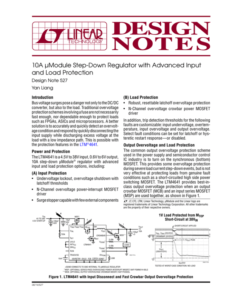
10A µModule Step-Down Regulator with Advanced Input and Load Protection Design Note 527 Yan Liang Introduction Bus voltage surges pose a danger not only to the DC/DC converter, but also to the load. Traditional overvoltage protection schemes involving a fuse are not necessarily fast enough, nor dependable enough to protect loads such as FPGAs, ASICs and microprocessors. A better solution is to accurately and quickly detect an overvoltage condition and respond by quickly disconnecting the input supply while discharging excess voltage at the load with a low impedance path. This is possible with the protection features in the LTM® 4641. Power and Protection The LTM4641 is a 4.5V to 38V input, 0.6V to 6V output, 10A step-down μModule ® regulator with advanced input and load protection options, including: (A) Input Protection • Undervoltage lockout, overvoltage shutdown with latchoff thresholds • N-Channel overvoltage power-interrupt MOSFET driver • Surge stopper capable with few external components (B) Load Protection • Robust, resettable latchoff overvoltage protection • N-Channel overvoltage crowbar power MOSFET driver In addition, trip detection thresholds for the following faults are customizable: input undervoltage, overtemperature, input overvoltage and output overvoltage. Select fault conditions can be set for latchoff or hysteretic restart response—or disabled. Output Overvoltage and Load Protection The common output overvoltage protection scheme used in the power supply and semiconductor control IC industry is to turn on the synchronous (bottom) MOSFET. This provides some overvoltage protection during severe load current step-down events, but is not very effective at protecting loads from genuine fault conditions such as a short-circuited high side power switching MOSFET. The LTM4641 provides best-inclass output overvoltage protection when an output crowbar MOSFET (MCB) and an input series MOSFET (MSP) are used together, as shown in Figure 1. L, LT, LTC, LTM, Linear Technology, µModule and the Linear logo are registered trademarks of Linear Technology Corporation. All other trademarks are the property of their respective owners. 4 VIN 4V TO 38V 4.5V START-UP + 1V Load Protected from MTOP Short-Circuit at 38VIN MSP* 10µF 50V ×2 100µF 50V 3 VING VINGP VINH MTOP VOUT VINL 750k CROWBAR MBOT fSET UVLO INTVCC DRVCC RUN TRACK/SS 10nF 1 SW VOSNS+ LTM4641 VOSNS– VOUT 1V 100µF 10A 2 MCB** ×3 4 VINL, VINH (25V/DIV) 5.49k 3 2 CROWBAR (5V/DIV) 5.49k 1.1VOUT PEAK LOAD VOUT (200mV/DIV) GND OVPGM IOVRETRY OVLO FCB LATCH SGND+ SHORT-CIRCUIT APPLIED DN527 F01a 1 5.6M +SGND CONNECTS TO GND INTERNAL TO µMODULE REGULATOR * MSP: (OPTIONAL) SERIES-PASS OVERVOLTAGE POWER INTERRUPT MOSFET, NXP PSMN014-60LS ** MCB: (OPTIONAL) OUTPUT OVERVOLTAGE CROWBAR MOSFET, NXP PH2625L 4µs/DIV TESTED AT WORST-CASE CONDITION: NO LOAD Figure 1. LTM4641 with Input Disconnect and Fast Crowbar Output Overvoltage Protection 06/14/527 DN527 F01b MSP is placed between the input power source (VIN) and the LTM4641's power stage input pins (VINH), and is used as a resettable electronic power-interrupt switch. When a fault condition, such as an output overvoltage (OOV) condition, is detected by the LTM4641’s internal circuitry, the gate of MSP is discharged within 2.6μs (maximum) and MSP turns off. The input source supply is thus disconnected from the LTM4641’s power stage input (VINH), preventing the hazardous (input) voltage from reaching the precious load. LTM4641 also uses an independent reference voltage to generate an OOV threshold, separate from the control IC’s bandgap voltage. Figure 1 shows the CROWBAR and VOUT waveforms when the top MOSFET MTOP fails, causing a shortcircuit between the VIN and SW nodes. CROWBAR goes high within 500ns and turns on MCB to short the output to ground. VOUT never exceeds 110% of the specified output voltage. Input Overvoltage and Undervoltage Protections The LTM4641 has input undervoltage and overvoltage protections, whose trip thresholds can be set by the user. Please refer to Figure 2. The UVLO pin feeds directly into the inverting input of a comparator whose trip threshold is 0.5V. When the UVLO pin falls below 0.5V, switching action is inhibited; when the UVLO pin exceeds 0.5V, switching action can resume. The IOVRETRY and OVLO pins each feed directly into noninverting inputs of comparators whose trip thresholds are 0.5V. When the IOVRETRY pin exceeds 0.5V, switching action is inhibited; when IOVRETRY falls below 0.5V, switching action can resume. When the OVLO pin exceeds 0.5V, switching action is inhibited; when OVLO subsequently falls below 0.5V, switching action cannot occur until the latch has Data Sheet Download www.linear.com/LTM4641 Linear Technology Corporation been reset. These three pins give added flexibility to tailor the behavior of the LTM4641. VIN + CIN(MLCC) 10µF ×2 CIN(BULK) VINH VINL RTUV RBUV RMOV UVLO < 0.5V = OFF UVLO RHYST HYST PULLS UP WHEN ON, HYST PULLS DOWN WHEN OFF RTOV IOVRETRY > 0.5V = OFF OVLO > 0.5V = LATCHOFF LTM4641 HYST IOVRETRY OVLO SGND RBOV GND AN527 F02 SGND CONNECTS TO GND INTERNAL TO MODULE. KEEP SGND ROUTES/PLANES SEPARATE FROM GND ON MOTHERBOARD Figure 2. Circuit to Set the Input UVLO, IOVRETRY and OVLO Thresholds Efficiency Figure 3 below shows the efficiency curves for the LTM4641 for a typical 12V input voltage for the circuit in Figure 1. With all the protection circuits, LTM4641 can still achieve high efficiency. 95 90 85 EFFICIENCY (%) MCB is an external optional crowbar device residing on VOUT. If the output voltage exceeds an adjustable threshold —default value is 11% above nominal— the LTM4641 pulls its CROWBAR output logic high immediately (500ns response time, maximum) and latches off its output voltage: the power stage becomes high impedance, with both internal top and bottom MOSFETs latched off. The CROWBAR output turns on MCB, discharging the output capacitors and preventing any further positive excursion of the output voltage. 80 6.0VOUT 5.0VOUT 3.3VOUT 2.5VOUT 1.8VOUT 1.5VOUT 1.2VOUT 1.0VOUT 0.9VOUT 75 70 65 60 0 1 2 3 4 5 6 7 8 OUTPUT CURRENT (A) 9 10 DN527 F03 Figure 3. Efficiency Curves of LTM4641 Conclusion The LTM4641 μModule regulator monitors input voltage, output voltage and temperature conditions. It can provide comprehensive electrical and thermal protection from excessive voltage stress for loads such as processors, ASICs and high end FPGAs. For applications help, call (408) 432-1900, Ext. 3979 dn527 LT/AP 0614 111K • PRINTED IN THE USA 1630 McCarthy Blvd., Milpitas, CA 95035-7417 (408) 432-1900 ● FAX: (408) 434-0507 ● www.linear.com LINEAR TECHNOLOGY CORPORATION 2014
