MX856/MX857
Single Driver for Attenuators
and GaAs FET Switches
INTEGRATED CIRCUITS DIVISION
Characteristics
Description
Parameter
Rating
Units
Output Voltage
20
V
Output Rise Time
5
ns
Output Fall Time
5
ns
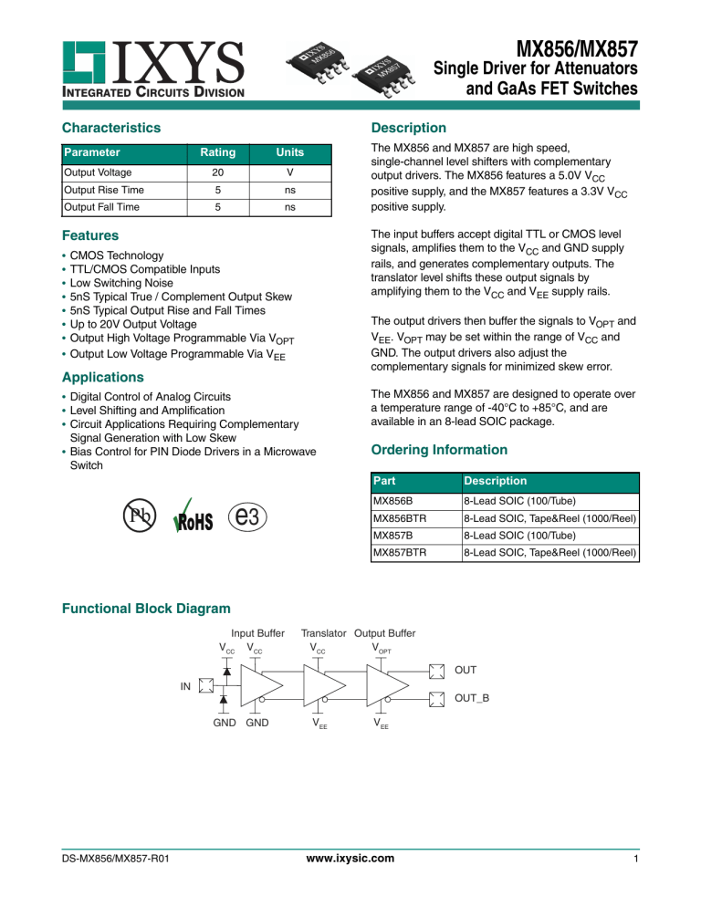
The MX856 and MX857 are high speed,
single-channel level shifters with complementary
output drivers. The MX856 features a 5.0V VCC
positive supply, and the MX857 features a 3.3V VCC
positive supply.
The input buffers accept digital TTL or CMOS level
signals, amplifies them to the VCC and GND supply
rails, and generates complementary outputs. The
translator level shifts these output signals by
amplifying them to the VCC and VEE supply rails.
Features
•
•
•
•
•
•
•
•
CMOS Technology
TTL/CMOS Compatible Inputs
Low Switching Noise
5nS Typical True / Complement Output Skew
5nS Typical Output Rise and Fall Times
Up to 20V Output Voltage
Output High Voltage Programmable Via VOPT
Output Low Voltage Programmable Via VEE
The output drivers then buffer the signals to VOPT and
VEE. VOPT may be set within the range of VCC and
GND. The output drivers also adjust the
complementary signals for minimized skew error.
Applications
• Digital Control of Analog Circuits
• Level Shifting and Amplification
• Circuit Applications Requiring Complementary
Signal Generation with Low Skew
• Bias Control for PIN Diode Drivers in a Microwave
Switch
e3
Pb
The MX856 and MX857 are designed to operate over
a temperature range of -40°C to +85°C, and are
available in an 8-lead SOIC package.
Ordering Information
Part
Description
MX856B
8-Lead SOIC (100/Tube)
MX856BTR
8-Lead SOIC, Tape&Reel (1000/Reel)
MX857B
8-Lead SOIC (100/Tube)
MX857BTR
8-Lead SOIC, Tape&Reel (1000/Reel)
Functional Block Diagram
Input Buffer
VCC VCC
Translator Output Buffer
VOPT
VCC
OUT
IN
OUT_B
GND GND
DS-MX856/MX857-R01
VEE
VEE
www.ixysic.com
1
MX856/MX857
INTEGRATED CIRCUITS DIVISION
1. Specifications . . . . . . . . . . . . . . . . . . . . . . . . . . . . . . . . . . . . . . . . . . . . . . . . . . . . . . . . . . . . . . . . . . . . . . . . . . . . . . . . . . . . . . . . . . . . . .
1.1 Package Pinout. . . . . . . . . . . . . . . . . . . . . . . . . . . . . . . . . . . . . . . . . . . . . . . . . . . . . . . . . . . . . . . . . . . . . . . . . . . . . . . . . . . . . . . .
1.2 Pin Description . . . . . . . . . . . . . . . . . . . . . . . . . . . . . . . . . . . . . . . . . . . . . . . . . . . . . . . . . . . . . . . . . . . . . . . . . . . . . . . . . . . . . . . .
1.3 Absolute Maximum Ratings . . . . . . . . . . . . . . . . . . . . . . . . . . . . . . . . . . . . . . . . . . . . . . . . . . . . . . . . . . . . . . . . . . . . . . . . . . . . . .
1.4 MX856: Guaranteed Operating Range . . . . . . . . . . . . . . . . . . . . . . . . . . . . . . . . . . . . . . . . . . . . . . . . . . . . . . . . . . . . . . . . . . . . . .
1.5 MX857: Guaranteed Operating Range . . . . . . . . . . . . . . . . . . . . . . . . . . . . . . . . . . . . . . . . . . . . . . . . . . . . . . . . . . . . . . . . . . . . . .
1.6 DC Electrical Characteristics . . . . . . . . . . . . . . . . . . . . . . . . . . . . . . . . . . . . . . . . . . . . . . . . . . . . . . . . . . . . . . . . . . . . . . . . . . . . .
1.7 ESD Warning . . . . . . . . . . . . . . . . . . . . . . . . . . . . . . . . . . . . . . . . . . . . . . . . . . . . . . . . . . . . . . . . . . . . . . . . . . . . . . . . . . . . . . . . .
1.8 AC Electrical Characteristics. . . . . . . . . . . . . . . . . . . . . . . . . . . . . . . . . . . . . . . . . . . . . . . . . . . . . . . . . . . . . . . . . . . . . . . . . . . . . .
3
3
3
3
4
4
4
5
5
2. Manufacturing Information . . . . . . . . . . . . . . . . . . . . . . . . . . . . . . . . . . . . . . . . . . . . . . . . . . . . . . . . . . . . . . . . . . . . . . . . . . . . . . . . . . . .
2.1 Moisture Sensitivity. . . . . . . . . . . . . . . . . . . . . . . . . . . . . . . . . . . . . . . . . . . . . . . . . . . . . . . . . . . . . . . . . . . . . . . . . . . . . . . . . . . . .
2.2 ESD Sensitivity . . . . . . . . . . . . . . . . . . . . . . . . . . . . . . . . . . . . . . . . . . . . . . . . . . . . . . . . . . . . . . . . . . . . . . . . . . . . . . . . . . . . . . . .
2.3 Reflow Profile . . . . . . . . . . . . . . . . . . . . . . . . . . . . . . . . . . . . . . . . . . . . . . . . . . . . . . . . . . . . . . . . . . . . . . . . . . . . . . . . . . . . . . . . .
2.4 Mechanical Dimensions . . . . . . . . . . . . . . . . . . . . . . . . . . . . . . . . . . . . . . . . . . . . . . . . . . . . . . . . . . . . . . . . . . . . . . . . . . . . . . . . .
6
6
6
6
7
2
www.ixysic.com
R01
MX856/MX857
INTEGRATED CIRCUITS DIVISION
1 Specifications
1.2 Pin Description
1.1 Package Pinout
OUT
1
8
OUT_B
Pin#
Name
1
OUT
Output Driver
2
GND
VCC
Ground
Input Buffer
3
Description
Positive Supply for Input Buffer
GND
2
7
GND
4
VCC
3
6
VOPT
5
IN
VEE
4
5
6
IN
VEE
VOPT
Positive Supply for Output Driver
7
GND
Ground
8
OUT_B
Negative Supply for Output Driver
Complementary Output Driver
1.3 Absolute Maximum Ratings
Parameter
Symbol
Min
Positive DC Supply Voltage
VCC
Max
Units
-0.4
6
V
Negative DC Supply Voltage
VEE
-17
0.4
V
Output Positive DC Supply Voltage
VOPT
-
6
V
Output Positive to Negative Supply Voltage VOPT -VEE
-0.4
20
V
Positive to Negative Supply Voltage
VCC-VEE
-0.4
14
V
Positive to Output Supply Voltage
VCC-VOPT
V
-0.4
VCC+0.4
DC Input Voltage
VIN
-0.4
VCC+0.4
V
DC Input Current
IIN
-10
10
A
°C
TA
-40
85
Storage Temperature
TSTG
-65
150
°C
ESD Sensitivity (Human Body Model)
ESD
1.0
-
kV
Operating Temperature
Absolute maximum electrical ratings are at 25°C
Absolute maximum ratings are stress ratings. Stresses in
excess of these ratings can cause permanent damage to
the device. Functional operation of the device at conditions
beyond those indicated in the operational sections of this
data sheet is not implied.
R01
www.ixysic.com
3
MX856/MX857
INTEGRATED CIRCUITS DIVISION
1.4 MX856: Guaranteed Operating Range
Parameter
Symbol
Min
Max
Units
Positive DC Supply Voltage
VCC
3
5.5
V
Negative DC Supply Voltage
VEE
-15
-4.5
V
Output Positive DC Supply Voltage
VOPT
0
5.5
V
Output Positive to Negative Supply Voltage
VOPT -VEE
7.5
20
V
Positive to Negative Supply Voltage
VCC-VEE
7.5
20
V
Positive to Output Supply Voltage
VCC-VOPT
0
VCC
V
Operating Temperature
TA
-40
85
°C
Input Rise and Fall Time
TR, TF
0
500
ns
Symbol
Min
Max
Units
Positive DC Supply Voltage
VCC
3
3.6
V
Negative DC Supply Voltage
VEE
-17
-4.5
V
Output Positive DC Supply Voltage
VOPT
0
3.6
V
Output Positive to Negative Supply Voltage
VOPT -VEE
7.5
20
V
Positive to Negative Supply Voltage
VCC-VEE
7.5
20
V
Positive to Output Supply Voltage
VCC-VOPT
0
VCC
V
Operating Temperature
TA
-40
85
°C
Input Rise and Fall Time
TR, TF
0
500
ns
1.5 MX857: Guaranteed Operating Range
Parameter
1.6 DC Electrical Characteristics
Over guaranteed operating range.
Parameter
Conditions
Symbol
Min
Typ
Max
Units
Input High Voltage
-
VIH
2
-
-
V
Input Low Voltage
-
VIL
-
-
0.8
V
Output High Voltage (IOH=1mA)
-
VOH
VOPT -0.1
-
-
V
Output Low Voltage (IOL=1mA)
-
VOL
-
-
VEE +0.1
V
Input Current (VIN=0.0 to VCC)
-
IIN
-10
-
10
A
Supply Current (VIN=0 or VCC)
VCC=3.3V
-
<1
-
-
<1
-
-
<1
-
-
<1
-
-
<1
-
-
<1
-
VCC=5V
Supply Current (VIN=0 or VCC)
VCC=3.3V
VCC=5V
Supply Current (VIN=0 or VCC)
VCC=3.3V
VCC=5V
4
www.ixysic.com
ICC
IEE
IOPT
A
R01
MX856/MX857
INTEGRATED CIRCUITS DIVISION
1.7 ESD Warning
ESD (electrostatic discharge) sensitive device. Electrostatic charges can readily accumulate on test equipment and
the human body in excess of 4000 Volts. This energy can discharge without detection. Although the MX856 / MX857
feature proprietary ESD protection circuitry, permanent damage may be sustained if subjected to high energy
electrostatic discharges. Proper ESD precautions are recommended to avoid performance degradation or loss of
functionality.
1.8 AC Electrical Characteristics
VCC=VOPT=3.3V, VEE=-16.75V or -4.5V, input rise and fall times 6ns, VIN=3.1V, VIL=0.2V, TA=-40°C to +85°C
VCC=VOPT=5V, VEE=-15V or -4.5V, input rise and fall times 6ns, VIN=4.8V, VIL=0.2V, TA=-40°C to +85°C
Parameter
Conditions
Symbol
VCC=3.5V
Propagation Delay (Low to High Input)
VCC=3.5V
VCC=3.5V
VCC=3.5V
VCC=3.5V
VCC=5.0V
Input Capacitance
-
-
24
29
-
20
29
-
20
29
-
5
9
-
4
9
-
5
8
-
4
8
-
5
10
-
5
10
-
-
15
CIN
90%
90%
50%
50%
10%
Thl
90%
OUT
pF
Tskew
Tphl
10%
Tplh
Tskew
Tphl
90%
50%
90%
50%
10%
10%
Thl
VEE
VOPT
Tlh
www.ixysic.com
VOPT
90%
50%
50%
10%
Tplh
R01
ns
10%
Tlh
OUTB
Units
6ns
VCC-0.2V
0.2V
29
TSKEW
6ns
IN
22
TTHL
VCC=5.0V
Delay Skew (Output A to Output B)
-
TTLH
VCC=5.0V
Output Fall Time (CLD=10pF)
Max
TPHL
VCC=5.0V
Output Rise Time (CLD=10pF)
Typ
TPLH
VCC=5.0V
Propagation Delay (High to Low Input)
Min
VEE
5
MX856/MX857
INTEGRATED CIRCUITS DIVISION
2 Manufacturing Information
2.1 Moisture Sensitivity
All plastic encapsulated semiconductor packages are susceptible to moisture ingression. IXYS Integrated
Circuits Division classified all of its plastic encapsulated devices for moisture sensitivity according to the
latest version of the joint industry standard, IPC/JEDEC J-STD-020, in force at the time of product
evaluation. We test all of our products to the maximum conditions set forth in the standard, and guarantee
proper operation of our devices when handled according to the limitations and information in that standard as well as
to any limitations set forth in the information or standards referenced below.
Failure to adhere to the warnings or limitations as established by the listed specifications could result in reduced
product performance, reduction of operable life, and/or reduction of overall reliability.
This product carries a Moisture Sensitivity Level (MSL) rating as shown below, and should be handled according to
the requirements of the latest version of the joint industry standard IPC/JEDEC J-STD-033.
Device
Moisture Sensitivity Level (MSL) Rating
MX856B / MX857B
MSL 1
2.2 ESD Sensitivity
This product is ESD Sensitive, and should be handled according to the industry standard
JESD-625.
2.3 Reflow Profile
This product has a maximum body temperature and time rating as shown below. All other guidelines of
J-STD-020 must be observed.
Pb
6
Device
Maximum Temperature x Time
MX856B / MX857B
260°C for 30 seconds
e3
www.ixysic.com
R01
MX856/MX857
INTEGRATED CIRCUITS DIVISION
2.4 Mechanical Dimensions
2.4.1 MX856B/MX857B 8-Lead SOIC Package
0.40 / 1.27
(0.016 / 0.050)
3.80 / 4.00*
(0.150 / 0.157)
5.80 / 6.20
(0.228 / 0.244)
1.55
(0.061)
5.40
(0.213)
PIN 1
1.27 BSC
(0.05 BSC)
0.33 / 0.51
(0.013 / 0.020)
0.25 / 0.50 @45º
(0.010 / 0.020 @45º)
0.60
(0.024)
0.19 / 0.25
(0.008 / 0.010)
4.80 / 5.00*
(0.189 / 0.197)
0º / 8º
Recommended PCB Land Pattern
0.10 / 0.25
(0.004 / 0.010)
1.35 / 1.75
(0.053 / 0.069)
0.53 REF
(0.021 REF)
1.27
(0.050)
Dimensions
mm MIN / mm MAX
(inches MIN / inches MAX)
NOTES: (Unless otherwise specified)
1. Controlling dimensions: millimeters.
2. Dimensions (*) do not include mold protrusions.
3. Molded package shall conform to JEDEC standard configuration MS-012 variation AA.
2.4.2 MX856BTR/MX857BTR Tape & Reel Dimensions
4.00 ± 0.10
(0.157 ± 0.004)
2.00 ± 0.10
(0.079 ± 0.004)
R0.5 TYP
(R0.02 TYP)
330.2 DIA.
(13.00 DIA.)
0.30 ± 0.05
(0.012 ± 0.002)
B
ø1.55 ± 0.05
(ø0.061 ± 0.002)
B0=5.20 ± 0.10
(B0=0.205 ± 0.004)
Top Cover
Tape Thickness
0.066 MAX.
(0.0026 MAX.)
5.50 ± 0.10
(0.217 ± 0.004)
3.40 REF
(0.134 REF)
A
1.80 ± 0.10
(0.071 ± 0.004)
K0=2.30 ± 0.10
(K0=0.091 ± 0.004)
Embossed Carrier
1.75 ± 0.10
(0.205 ± 0.069)
Section B-B
12.00 ± 0.30
(0.472 ± 0.012)
A
8.00 ± 0.10
(0.315 ± 0.004)
B
ø1.50 MIN
(ø0.059 MIN)
A0=6.40 ± 0.10
(A0=0.252 ± 0.004)
4.70 REF
(0.185 REF)
1.20 REF
(0.047 REF)
70º
Embossment
DIMENSIONS
mm
(inches)
NOTES:
1. A0 and B0 measured at 0.3mm above base of pocket.
2. 10 pitches cumulative tol. ±0.2mm.
Section A-A
For additional information please visit our website at: www.ixysic.com
IXYS Integrated Circuits Division makes no representations or warranties with respect to the accuracy or completeness of the contents of this publication and reserves the right to make
changes to specifications and product descriptions at any time without notice. Neither circuit patent licenses nor indemnity are expressed or implied. Except as set forth in IXYS Integrated
Circuits Division’s Standard Terms and Conditions of Sale, IXYS Integrated Circuits Division assumes no liability whatsoever, and disclaims any express or implied warranty, relating to its
products including, but not limited to, the implied warranty of merchantability, fitness for a particular purpose, or infringement of any intellectual property right.
The products described in this document are not designed, intended, authorized or warranted for use as components in systems intended for surgical implant into the body, or in other
applications intended to support or sustain life, or where malfunction of IXYS Integrated Circuits Division’s product may result in direct physical harm, injury, or death to a person or severe
property or environmental damage. IXYS Integrated Circuits Division reserves the right to discontinue or make changes to its products at any time without notice.
Specification: DS-MX856/MX857-20110729
©Copyright 2012, IXYS Integrated Circuits Division
All rights reserved. Printed in USA.
12/22/2012
R01
www.ixysic.com
7


