The Design of SiGe HBT Direct
advertisement
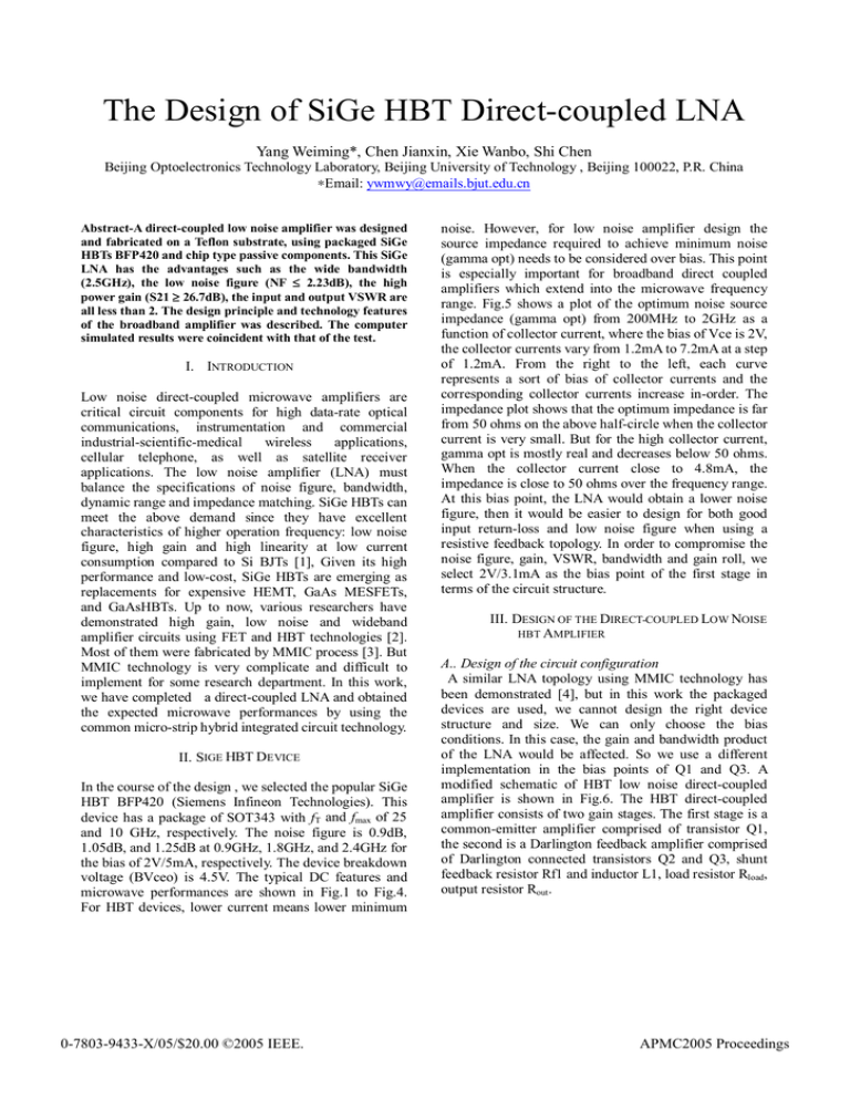
The Design of SiGe HBT Direct-coupled LNA Yang Weiming*, Chen Jianxin, Xie Wanbo, Shi Chen Beijing Optoelectronics Technology Laboratory, Beijing University of Technology , Beijing 100022, P.R. China ∗Email: ywmwy@emails.bjut.edu.cn Abstract-A direct-coupled low noise amplifier was designed and fabricated on a Teflon substrate, using packaged SiGe HBTs BFP420 and chip type passive components. This SiGe LNA has the advantages such as the wide bandwidth (2.5GHz), the low noise figure (NF ≤ 2.23dB), the high power gain (S21 ≥ 26.7dB), the input and output VSWR are all less than 2. The design principle and technology features of the broadband amplifier was described. The computer simulated results were coincident with that of the test. I. INTRODUCTION Low noise direct-coupled microwave amplifiers are critical circuit components for high data-rate optical communications, instrumentation and commercial industrial-scientific-medical wireless applications, cellular telephone, as well as satellite receiver applications. The low noise amplifier (LNA) must balance the specifications of noise figure, bandwidth, dynamic range and impedance matching. SiGe HBTs can meet the above demand since they have excellent characteristics of higher operation frequency: low noise figure, high gain and high linearity at low current consumption compared to Si BJTs [1], Given its high performance and low-cost, SiGe HBTs are emerging as replacements for expensive HEMT, GaAs MESFETs, and GaAsHBTs. Up to now, various researchers have demonstrated high gain, low noise and wideband amplifier circuits using FET and HBT technologies [2]. Most of them were fabricated by MMIC process [3]. But MMIC technology is very complicate and difficult to implement for some research department. In this work, we have completed a direct-coupled LNA and obtained the expected microwave performances by using the common micro-strip hybrid integrated circuit technology. II. SIGE HBT DEVICE In the course of the design , we selected the popular SiGe HBT BFP420 (Siemens Infineon Technologies). This device has a package of SOT343 with fT and fmax of 25 and 10 GHz, respectively. The noise figure is 0.9dB, 1.05dB, and 1.25dB at 0.9GHz, 1.8GHz, and 2.4GHz for the bias of 2V/5mA, respectively. The device breakdown voltage (BVceo) is 4.5V. The typical DC features and microwave performances are shown in Fig.1 to Fig.4. For HBT devices, lower current means lower minimum 0-7803-9433-X/05/$20.00 ©2005 IEEE. noise. However, for low noise amplifier design the source impedance required to achieve minimum noise (gamma opt) needs to be considered over bias. This point is especially important for broadband direct coupled amplifiers which extend into the microwave frequency range. Fig.5 shows a plot of the optimum noise source impedance (gamma opt) from 200MHz to 2GHz as a function of collector current, where the bias of Vce is 2V, the collector currents vary from 1.2mA to 7.2mA at a step of 1.2mA. From the right to the left, each curve represents a sort of bias of collector currents and the corresponding collector currents increase in-order. The impedance plot shows that the optimum impedance is far from 50 ohms on the above half-circle when the collector current is very small. But for the high collector current, gamma opt is mostly real and decreases below 50 ohms. When the collector current close to 4.8mA, the impedance is close to 50 ohms over the frequency range. At this bias point, the LNA would obtain a lower noise figure, then it would be easier to design for both good input return-loss and low noise figure when using a resistive feedback topology. In order to compromise the noise figure, gain, VSWR, bandwidth and gain roll, we select 2V/3.1mA as the bias point of the first stage in terms of the circuit structure. III. DESIGN OF THE DIRECT-COUPLED LOW NOISE HBT AMPLIFIER A.. Design of the circuit configuration A similar LNA topology using MMIC technology has been demonstrated [4], but in this work the packaged devices are used, we cannot design the right device structure and size. We can only choose the bias conditions. In this case, the gain and bandwidth product of the LNA would be affected. So we use a different implementation in the bias points of Q1 and Q3. A modified schematic of HBT low noise direct-coupled amplifier is shown in Fig.6. The HBT direct-coupled amplifier consists of two gain stages. The first stage is a common-emitter amplifier comprised of transistor Q1, the second is a Darlington feedback amplifier comprised of Darlington connected transistors Q2 and Q3, shunt feedback resistor Rf1 and inductor L1, load resistor Rload, output resistor Rout. APMC2005 Proceedings Fig.1. The DC characteristics of BFP420 Fig.4. The S12 of BFP420 Fig.2. The minimum noise figure of BFP420 Fig.5. Gamma opt. versus device collector current Fig.3. The S21 of BFP420 Where the transistor Q4 act as a bias resistor with the base and collector connected together. The first stage acts as a low noise common-emitter amplifier which determines the overall amplifier noise figure. The second stage Darlington feedback amplifier provides wideband gain and output drive capability. The gain-bandwidth characteristics of the Darlington feedback stage can be optimized by Rf1 without degrading the noise figure of the overall amplifier. Rf1 also provides a current source for biasing transistor Q1 of the first stage. The shunt inductor L1 and the serial inductor L2 of emitter are used to compensate the high frequency response of the amplifier so as to improve the flatness within the effective bandwidth. The bias resistor Rb2 act as an assistant of Rf1, the load resistor Rload and output resistor Rout were employed to adjust the output VSWR. By using the bias transistor Q4 to replace the traditional bias resistor, a higher gain and better bias stability under large signal condition can be obtained [5]. The shunt feedback resistor, Rf2, connected between the emitter of Q2 and the base of Q1, can be adjusted to change the effective impedance looking out of the base of Q1 toward the source, and therefore, optimized for minimum noise match. In addition, Rf2 provides RF shunt feedback, which impacts the gain-bandwidth response and determines the input impedance match of the amplifier to 50Ω. Thus Rf1, L1, L2, Rf2, Rload and Rout can be adjusted in order to obtain an optimal combination of gain, noise figure, input VSWR, and output VSWR. B. Computer simulation The schematic of the SiGe HBT LNA was designed by ADS2003C software platform. The passive component parameters, the micro-strip line structure, and the ground design were optimized by the layout simulation tools. When collector emitter voltage (Vce) was 2V, and collector emitter current (Ice) was 3.1mA for Q1, Vce is 2.3V and 3.3v, Ice is 4.2mA and 4.4mA for Q2 and Q3, respectively. The simulation results are shown in Fig.7 to Fig.12. The simulated performances of LNA are as follows: S21=27.5dB, BW=2.5GHz, input VSWR=1∼1.77, output VSWR=1∼1.97, NF≤2.2dB, P1dB=3dBm. Pass-band ripple < ± 0.5dB. Fig.9. The simulated S12 of LNA. Fig.6. The topology structure of the LNA Fig.10. The simulated input VSWR of the LNA. Fig.7. The simulated noise figure of LNA. Fig.11. The simulated output VSWR of the LNA Fig.8. The simulated S21 of LNA. Fig.12. The simulated P1dB of LNA IV. IMPLEMENTATION AND MEASUREMENT RESULTS The designed LNA was fabricated and mounted on a Teflon substrate (εr = 2.52, conductor thickness = 0.018mm, substrate height is 0.54mm), using four packaged SiGe HBTs BFP420 (Infineon technology) and chip type passive components, some small passive components were implemented by micro-strip lines. The corresponding components were all connected by micro-strip lines. The back of the substrate was covered with copper with some small vias every certain space away, which were connected to the ground, and then fixed in a shield box. The supply voltage was 4.5V with a filter circuit to decrease the noise of the power. This LNA circuit need not other passive match components, only two large DC-block capacitors are needed at the input port and the output port respectively. The noise figure was tested by HP8970B, HP8971C, HP8350. The small signal features of the fabricated LNA was measured by network analyzer (HP8753). The typical gain of the SiGe HBT LNA was 27dB, the bandwidth is 2.5GHz, and the noise figure is 2.2dB or so. The main measured results are shown in Table I. we can see that the measured results are close to that of the simulation. TABLE I THE MEASURED RESULTS OF LOW NOISE AMPLIFIER 100MHz 2.5GHz S21 S12 Input VSWR Output VSWR NF 27.05dB 26.62dB -39.20dB 1.05 1.46 2.19 -37.84dB 1.80 1.96 2.23 V. CONCLUSION A SiGe HBT direct coupled LNA was designed using the microwave simulation tool ADS2003C. The LNA was implemented on a Teflon substrate using packaged SiGe HBTs BFP420 and chip type passive components in hybrid microwave circuit technology. Compared to the LNA using MMIC technology, this LNA topology has some modification. The feedback inductor has been used to compensate the high frequency response and improve the bandwidth. The replacement of the bias resistor by the bias transistor can obtain a larger gain. The bias resistor Rb2 act as an assistant of Rf1 to adjust the input VSWR and bandwidth. This SiGe LNA resulted in a noise figure of 2.2dB, and 27dB gain over 0 to 2.5 GHz range. The input and output VSWR are all less than 2. The amplifier uses a direct-coupled topology to achieve wideband frequency performances from base-band to L-band. This sort of LNA is useful for instrumentation and commercial industrial-scientific-medical wireless applications, cellular telephone and electro-optical communication applications. ACKNOWLEDGEMENT This work has been supported by Beijing Natural Science Fund of China, grant No. is 4032005. REFERENCES [1] Y. Suzuki, H. Shimawaki, Y. Amamiya, N.Nagono, T. Niws, H. Yano, and K. Honjo, “50-GHz bandwidth baseband amplifiers using GaAs-based HBTs,” Journal of Solid State Circuits, vol. 33, pp.1336-1341, 1998 [2] H. Knapp, D. Zoscbg, T. Meister, K, Kufinger, S. Boguth, and L. Treitinger, “15 GHz wideband amplifier with 2.8 dB noise figure in SiGe bipolar technology,” 2001 Radio Frequency Integrated Circuits Symposition Digest of Papers,2001 [3] Virdee, A. S, “Computer-aided design of ultra-broadband 100MHz to 20 GHz amplifier,” Microwave Journal, 2000(2): pp.77-88 [4] K. W. Kobayashi and A. K. Oki, “Sub-2.5 dB noise figure GaAs HBT direct-coupled LNA’s for high volume commercial applications to 6 GHz,” IEEE GaAs IC Symp. Dig., Philadelphia, PA, Oct. 1994, pp. 303-306 [5] T. K. Lee, W. S. Chan, and Y.M. Siu, “Darlington feedback amplifier with good bias stability under large-signal conditions,” Electronics Letters 30th September 2004, Vol.40, No. 20
