ECMF02-4CMX8
Common mode filter with ESD protection for USB 2.0 interface
Datasheet production data
Applications
Where transient overvoltage protection in ESD
sensitive equipment is required, such as:
Computers
Printers
Communication systems
Cellular phone handsets and accessories
Video equipment
0LFUR4)1/
SLQYLHZ
Description
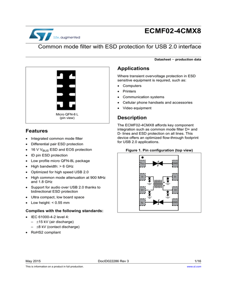
The ECMF02-4CMX8 affords key component
integration such as common mode filter D+ and
D- lines and ESD protection on all lines. This
device offers an optimized flow-through footprint
for USB 2.0 applications.
Features
Integrated common mode filter
Differential pair ESD protection
16 V VBUS ESD and EOS protection
Figure 1. Pin configuration (top view)
ID pin ESD protection
Low profile micro QFN-8L package
High bandwidth: > 6 GHz
9%86
*1'
'
'
'
'
,'
*1'
Optimized for high speed USB 2.0
High common mode attenuation at 900 MHz
and 1.8 GHz
Support for audio over USB 2.0 thanks to
bidirectional ESD protection
Ultra compact, low board space
Low height: < 0.55 mm
Complies with the following standards:
IEC 61000-4-2 level 4:
– 15 kV (air discharge)
– 8 kV (contact discharge)
RoHS2 compliant
May 2015
This is information on a product in full production.
DocID022286 Rev 3
1/16
www.st.com
Characteristics
1
ECMF02-4CMX8
Characteristics
Table 1. Absolute maximum ratings (Tamb = 25 °C)
Symbol
Parameter
Value
ESD discharge IEC 61000-4-2, level 4
Contact discharge on D+/D- pins
Contact discharge on VBUS and ID pins
Air discharge on all pins
Unit
10
20
30
VPP
Peak pulse voltage(1)
PPP
Peak pulse power (8/20µs) on VBUS
150
W
IPP
Peak pulse current (8/20µs) on VBUS
4.8
A
Tj
Maximum operating junction temperature
-40 to +125
°C
Storage temperature range
-55 to +150
°C
Tstg
kV
1. Measurements done on IEC 61000-4-2 test bench. For further details see Application note AN3353.
Figure 2. Electrical characteristics - definitions
,
6\PERO
3DUDPHWHU
9%5
,50
950
9&/
,33
,5
%UHDNGRZQYROWDJH
/HDNDJHFXUUHQW# 950
6WDQGRII YROWDJH
&ODPSLQJYROWDJH
3HDNSXOVHFXUUHQW
%UHDNGRZQFXUUHQW
,33
9&/ 9%5
950
,5
,50
,50
,5
,33
2/16
DocID022286 Rev 3
9
950 9%5 9&/
ECMF02-4CMX8
Characteristics
Table 2. Electrical characteristics (values, Tamb = 25 °C)
Symbol
Test conditions
Min.
Typ.
Max.
Unit
Data lines
VBR
IR = 1 mA
IRM
VRM = 5.5 V per line
RDC
DC serial resistance on data line
6
V
100
nA
3
4
Ω
16.5
18
V
VBUS
VBR
IR = 1 mA
15
IRM
VRM = 12 V
50
nA
VCL
Clamping voltage. IPP = 1 A, tp = 8/20 µs
20
V
VCL
Clamping voltage. IPP = 2.5 A, tp = 8/20 µs
24
V
ID
VBR
IR = 1 mA
IRM
VRM = 1.5 V per line
6
V
100
DocID022286 Rev 3
nA
3/16
16
Characteristics
ECMF02-4CMX8
Figure 3. SDD21 differential attenuation measurement (Z0 diff = 90 Ω ) for data lines D+ and D6''G%
)+]
N
0
0
0
*
Figure 4. SCC21 common mode attenuation measurement (Z0 com = 45 Ω )
6&&G%
)+]
N
4/16
0
0
0
DocID022286 Rev 3
*
ECMF02-4CMX8
Characteristics
Figure 5. ID frequency response measurement (Z0 = 75 Ω )
6G%
)+]
N
0
0
0
*
Figure 6. Differential (ZDD21) and common mode (ZCC21) impedance versus frequency
(
=''DQG=&&ȍ
(
(
(
(
=''
(
=&&
DocID022286 Rev 3
(
(
5/16
16
Characteristics
ECMF02-4CMX8
Figure 7. ESD test conditions
9%86
*1'
$WWHQXDWRUV
'
'
G%
'
'
,'
*1'
G%
2VFLOORVFRSH
:
Figure 8. ESD response to IEC 61000-4-2 (+8 kV contact discharge) on VBUS
933 (6'SHDNYROWDJH
9&/ FODPSLQJYROWDJH#QV
9&/ FODPSLQJYROWDJH#QV
9&/ FODPSLQJYROWDJH#QV
9
9
9
6/16
DocID022286 Rev 3
9
ECMF02-4CMX8
Characteristics
Figure 9. ESD response to IEC 61000-4-2 (-8 kV contact discharge) on VBUS
9
9
9
9
933 (6'SHDNYROWDJH
9&/ FODPSLQJYROWDJH#QV
9&/ FODPSLQJYROWDJH#QV
9&/ FODPSLQJYROWDJH#QV
Figure 10. ESD response to IEC 61000-4-2 (+8 kV contact discharge) on ID
933 (6'SHDNYROWDJH
9&/ FODPSLQJYROWDJH#QV
9&/ FODPSLQJYROWDJH#QV
9&/ FODPSLQJYROWDJH#QV
9
9
9
DocID022286 Rev 3
9
7/16
16
Characteristics
ECMF02-4CMX8
Figure 11. ESD response to IEC 61000-4-2 (-8 kV contact discharge) on ID
9
9
9
9
933 (6'SHDNYROWDJH
9&/ FODPSLQJYROWDJH#QV
9&/ FODPSLQJYROWDJH#QV
9&/ FODPSLQJYROWDJH#QV
Figure 12. ESD response to IEC 61000-4-2 (+8 kV contact discharge) on differential lane
933 (6'SHDNYROWDJH
9&/ FODPSLQJYROWDJH#QV
9&/ FODPSLQJYROWDJH#QV
9&/ FODPSLQJYROWDJH#QV
9
9
9
8/16
DocID022286 Rev 3
9
ECMF02-4CMX8
Characteristics
Figure 13. ESD response to IEC 61000-4-2 (-8 kV contact discharge) on differential lane
9
9
9
9
933 (6'SHDNYROWDJH
9&/ FODPSLQJYROWDJH#QV
9&/ FODPSLQJYROWDJH#QV
9&/ FODPSLQJYROWDJH#QV
Figure 14. Eye diagram (loaded by Zdiff = 90 ) Figure 15. Eye diagram (loaded by Zdiff = 90 )
with USB2.0 [mask 1] board only
with USB2.0 [mask 1] board with ECM02-4CMX8
5LVHWLPHSV )DOOWLPHSV
(\HKHLJKWPY
(\HZLGWKQV
5LVHWLPHSV )DOOWLPHSV
DocID022286 Rev 3
(\HKHLJKWPY
(\HZLGWKQV
9/16
16
Characteristics
ECMF02-4CMX8
Figure 16. TDR measurement (loaded by Zdiff = 90 ), rise time 400 ps
=GLII:
WQV
Figure 17. HS sync
10/16
DocID022286 Rev 3
ECMF02-4CMX8
Characteristics
Figure 18. Total harmonic distortion on differential lanes
Figure 19. Crosstalk on differential lanes
DocID022286 Rev 3
11/16
16
Application schematic
2
ECMF02-4CMX8
Application schematic
Figure 20. Application schematic
9%86
*1'
'
'
'
'
,'
*1'
0LFUR86%
UHFHSWDFOH
12/16
DocID022286 Rev 3
7RZDUGV86%WUDQVFHLYHU
(&0)&0;
ECMF02-4CMX8
3
Package information
Package information
Epoxy meets UL94, V0
Lead-free packages
In order to meet environmental requirements, ST offers these devices in different grades of
ECOPACK® packages, depending on their level of environmental compliance. ECOPACK®
specifications, grade definitions and product status are available at: www.st.com.
ECOPACK® is an ST trademark.
Micro QFN-8L package information
Figure 21. Micro QFN-8L package outline
'
$
$
(
H
E
3,1
/
3.1
Table 3. Micro QFN-8L package mechanical data
Dimensions
Ref.
Inches(1)
Millimeters
Typ.
Min.
Max.
Typ.
Min.
Max.
A
0.50
0.45
0.55
0.020
0.018
0.022
A1
0.02
0.00
0.05
0.0008
0.00
0.002
b
0.20
0.15
0.25
0.008
0.006
0.010
D
2.50
2.45
2.55
0.098
0.096
0.100
E
1.20
1.15
1.25
0.047
0.045
0.049
DocID022286 Rev 3
13/16
16
Package information
ECMF02-4CMX8
Table 3. Micro QFN-8L package mechanical data (continued)
Dimensions
Ref.
Inches(1)
Millimeters
Typ.
Min.
Max.
Typ.
Min.
Max.
e
0.50
0.45
0.55
0.020
0.018
0.022
L
0.40
0.30
0.50
0.016
0.012
0.020
1. Values in inches are converted from mm and rounded to 4 decimal digits.
Figure 22. Footprint
Figure 23. Marking
;;
::
<3
'RW3LQ
;;0DUNLQJ
::$VVHPEO\ZHHN
<$VVHPEO\\HDU
3$VVHPEO\SODQW
Figure 24. Tape and reel specifications
'RWLGHQWLI\LQJ3LQ $ORFDWLRQ
s s s s s s s
s s s $OOGLPHQVLRQVDUHW\SLFDO YDOXHVLQPP
Note:
14/16
8VHUGLUHFWLRQRIXQUHHOLQJ
More packing information is available in the application notes: AN1751: “EMI Filters:
Recommendations and measurements”
DocID022286 Rev 3
ECMF02-4CMX8
4
Ordering information
Ordering information
Figure 25. Ordering information scheme
(&0)&0;
)XQFWLRQ
(6'FRPPRQPRGHILOWHU
1XPEHU RI OLQHV
OLQHV
1XPEHU RI (6' SURWHFWHG OLQHV
(6'SURWHFWHGOLQHV
9HUVLRQ
& 99%5 IRU9%86
3DFNDJH
0; 0LFUR4)1/
Table 4. Ordering information
Order code
Marking
Package
Weight
Base qty
Delivery mode
ECMF02-4CMX8
KG
Micro QFN-8L
3.7 mg
3000
Tape and reel
For the latest information on available order codes see the product pages on: www.st.com.
5
Revision history
Table 5. Document revision history
Date
Revision
Changes
19-Sep-2012
1
Initial release.
27-May-2014
2
Updated Figure 24, Figure 25 and reformatted the document.
05-May-2015
3
Added Figure 6.
Updated Table 1.
Format updated to current standard.
DocID022286 Rev 3
15/16
16
ECMF02-4CMX8
IMPORTANT NOTICE – PLEASE READ CAREFULLY
STMicroelectronics NV and its subsidiaries (“ST”) reserve the right to make changes, corrections, enhancements, modifications, and
improvements to ST products and/or to this document at any time without notice. Purchasers should obtain the latest relevant information on
ST products before placing orders. ST products are sold pursuant to ST’s terms and conditions of sale in place at the time of order
acknowledgement.
Purchasers are solely responsible for the choice, selection, and use of ST products and ST assumes no liability for application assistance or
the design of Purchasers’ products.
No license, express or implied, to any intellectual property right is granted by ST herein.
Resale of ST products with provisions different from the information set forth herein shall void any warranty granted by ST for such product.
ST and the ST logo are trademarks of ST. All other product or service names are the property of their respective owners.
Information in this document supersedes and replaces information previously supplied in any prior versions of this document.
© 2015 STMicroelectronics – All rights reserved
16/16
DocID022286 Rev 3


