MP8130
Ultra Low Power
36V, 200KHz, High Voltage Op Amp
The Future of Analog IC Technology
DESCRIPTION
FEATURES
The MP8130 is a rail-to-rail output, high voltage
operational amplifier in a TSOT-23 package.
This amplifier provides 200KHz bandwidth while
consuming an incredibly low 10µA of supply
current. The MP8130 can operate over a single
supply range of 2.7V to 36V. It is available in
tiny TSOT23-5 packages.
•
•
•
•
•
•
•
•
•
Single Supply Operation: 2.7V to 36V
TSOT23-5 Package
200KHz –3dB Bandwidth
10µA Supply Current
Rail-to-Rail Output
Unity-Gain Stable
Input Common Mode to Ground
Drives Up to 1000pF of Capacitive Loads
Available in a TSOT23-5 Package
APPLICATIONS
•
•
•
Precision Micropower Amplifiers
Micropower Signal Processing
Test Equipment
“MPS” and “The Future of Analog IC Technology” are Registered Trademarks of
Monolithic Power Systems, Inc.
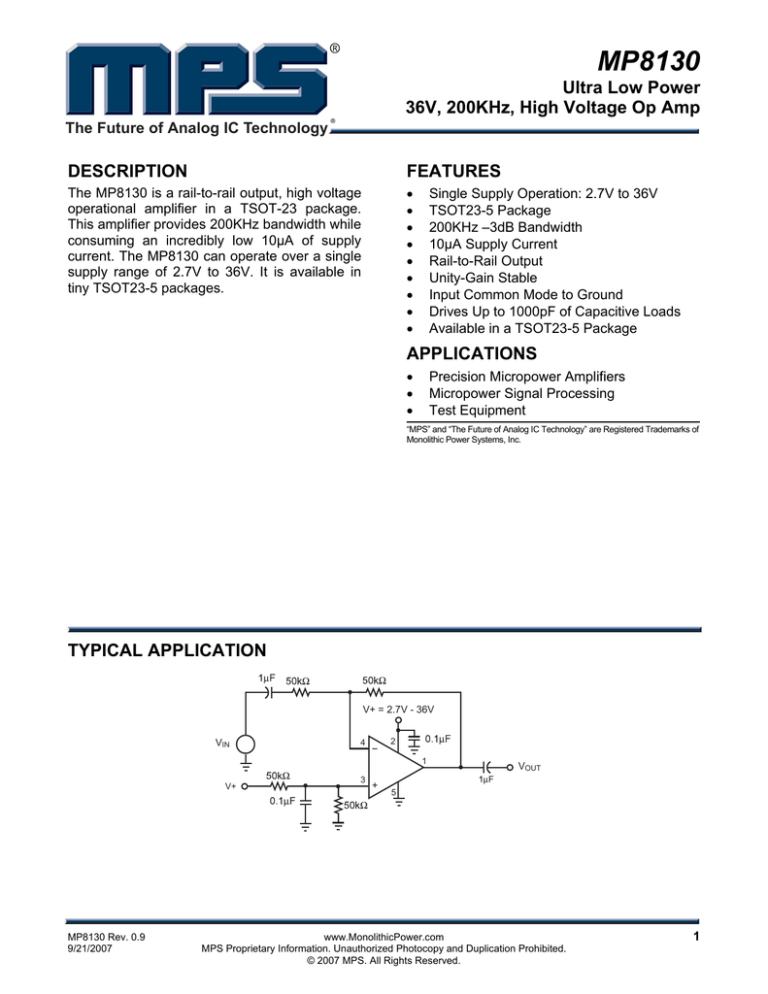
TYPICAL APPLICATION
V+ = 2.7V - 36V
VIN
4
--
2
1
V+
MP8130 Rev. 0.9
9/21/2007
3
+
VOUT
5
www.MonolithicPower.com
MPS Proprietary Information. Unauthorized Photocopy and Duplication Prohibited.
© 2007 MPS. All Rights Reserved.
1
MP8130 – ULTRA LOW POWER, 36V, 200KHZ, HIGH VOLTAGE OP AMP
ABSOLUTE MAXIMUM RATINGS (1)
PACKAGE REFERENCE
Supply Voltage (V+ to V-) ....................... +40.0V
Differential Input Voltage (VIN+ – VIN–) ....... +6.0V
Input Voltage
VIN+ = VIN–...................... (V-) – 0.3V, (V+) + 0.3V
TOP VIEW
OUT
1
V+
2
IN+
3
5
V-
Recommended Operating Conditions
4
Supply Voltage ............................ +2.7V to +36V
Operating Temperature .............–40°C to +85°C
IN-
Thermal Resistance
Part Number*
Package
Temperature
MP8130DJ
TSOT23-5
–40°C to +85°C
*
(2)
For Tape & Reel, add suffix –Z (eg. MP8130DJ–Z)
For RoHS compliant packaging, add suffix –LF (eg.
MP8130DJ–LF–Z)
(3)
θJA
θJC
TSOT23-5.............................. 220 .... 110.. °C/W
Notes:
1) Exceeding these ratings may damage the device.
2) The device is not guaranteed to function outside of its
operating conditions.
3) Measured on approximately 1” square of 1 oz copper.
ELECTRICAL CHARACTERISTICS
V+ = +20V, V– = 0V, VCM = V+/2, RL = 50kΩ, TA = +25°C, unless otherwise noted.
Parameter
Symbol Condition
Input Offset Voltage
Input Offset Voltage Temp
Coefficient
Input Bias Current (4)
Input Offset Current (4)
Input Voltage Range
Common-Mode Rejection
Ratio
Power Supply Rejection
Ratio
Large Signal Voltage Gain
Maximum Output Voltage
Swing
Minimum Output Voltage
Swing
Gain-Bandwidth Product (4)
Min
Typ
Max
Units
–5
1
+5
mV
VOS
IB
IOS
VCM
CMRR
PSRR
AVOL
CMRR > 60dB (V+ = 36V)
0
0 < VCM < 36.0V (V+ = 36V)
80
Supply Voltage change of
2.7V/ 36V
RL = 100kΩ,
VOUT = 5.0 Peak to Peak
60
15
µV/°C
2
0.2
pA
pA
V
36
82
dB
80
dB
88
dB
VOUT
RL = 100k
(V+) – 50mV
V
VOUT
RL = 100k
(V–) + 50mV
V
100
KHz
200
KHz
0.1
V/µs
10
mA
mA
µA
GBW
–3dB Bandwidth (4)
BW
Slew Rate (4)
SR
Short Circuit Current
ISC
Supply Current
Isup
RL = 1MΩ,CL = 2pF,
VOUT = 0V
AV = 1, CL = 2pF,
RL = 1MΩ
AV = 1, CL = 2pF,
RL = 1MΩ
Source
Sink
No Load
-20
20
15
Note:
4) Guaranteed by design.
MP8130 Rev. 0.9
9/21/2007
www.MonolithicPower.com
MPS Proprietary Information. Unauthorized Photocopy and Duplication Prohibited.
© 2007 MPS. All Rights Reserved.
2
MP8130 – ULTRA LOW POWER, 36V, 200KHZ, HIGH VOLTAGE OP AMP
TYPICAL PERFORMANCE CHARACTERISTICS
C1= C3 =0.1μF, C2=C4=10μF, RL = 1MΩ (Reference Figure 3)
Output Voltage vs.
Output Current
Output Voltage vs.
Output Current
Sourcing
Sinking
V+=20V
V- =20V
0
20
40
60
80
OUTPUT CURRENT (mA)
Sinking
0.5
1.0
1.5
2.0
SUPPLY VOLTAGE (V)
OUTPUT CURRENT (mA)
Gain
1
50
Offset Voltage vs.
Common Mode Voltage
-225
1000
50
225
40
180
Phase
20
90
0
0
-10
-45
Gain
V+=10V
V- =10V
-40
-50
1.0
1.5
2.0
2.5
SUPPLY VOLTAGE (V)
135
45
10
-30
V+=20V
V- =20V
0.5
-180
10
100
FREQUENCY (KHz)
-20
0
-90
-135
V+=10V
V- =10V
30
0
2.5
-45
Gain Bandwidth and
Phase Margin
100
0
0
-10
-50
20
40
60
80
100
OUTPUT CURRENT (mA)
Sourcing
V+=20V
V- =20V
45
0
-40
Short Circuit Current vs.
Supply Voltage
50
90
Offset Voltage vs.
Supply Voltage
1
10
100
FREQUENCY (KHz)
PHASE
OUTPUT CURRENT (mA)
0
135
10
-30
V+=20V
V- =20V
180
20
-20
Short Circuit Current vs.
Supply Voltage
100
0
10
0
100
Phase
30
GAIN (dB)
0
40
GAIN (dB)
OUTPUT VOLTAGE (V)
10
225
50
20
PHASE
OUTPUT VOLTAGE (V)
20
Gain Bandwidth and
Phase Margin
-90
-135
-180
-225
1000
PSRR
100
-1.2
-1.84
-2.38
-2.92
-3.46
-4.00
V+=10V
V- =10V
0
1
2
3
4
5
COMMON MODE VOLTAGE (V)
MP8130 Rev. 0.9
9/21/2007
90
80
-1.3
PSRR (dB)
OFFSET VOLTAGE (mV)
OFFSET VOLTAGE (mV)
-1.30
-1.4
-1.5
70
60
50
40
30
-1.6
-1.7
20
V+=10V
V- =10V
0
1
2
3
4
SUPPLY VOLTAGE (V)
10
5
0
0.1
V+=10V
V- =10V
1
10
100 1000 10000
FREQUENCY (KHz)
www.MonolithicPower.com
MPS Proprietary Information. Unauthorized Photocopy and Duplication Prohibited.
© 2007 MPS. All Rights Reserved.
3
MP8130 – ULTRA LOW POWER, 36V, 200KHZ, HIGH VOLTAGE OP AMP
TYPICAL PERFORMANCE CHARACTERISTICS
C1= C3 =0.1μF, C2=C4=10μF, RL = 1MΩ (Reference Figure 3)
VIN
0.2V/div.
VIN
0.2V/div.
VIN
0.2V/div.
VO
0.2V/div.
VO
0.2V/div.
VO
0.2V/div.
VIN
0.1V/div.
VIN
0.1V/div.
VIN
0.2V/div.
VO
0.5V/div.
VO
1V/div.
VO
0.1V/div.
VIN
0.2V/div.
VIN
0.2V/div.
VO
0.2V/div.
VIN
0.1V/div.
VO
0.5V/div.
VO
0.5V/div.
MP8130 Rev. 0.9
9/21/2007
www.MonolithicPower.com
MPS Proprietary Information. Unauthorized Photocopy and Duplication Prohibited.
© 2007 MPS. All Rights Reserved.
4
MP8130 – ULTRA LOW POWER, 36V, 200KHZ, HIGH VOLTAGE OP AMP
TYPICAL PERFORMANCE CHARACTERISTICS
C1= C3 =0.1μF, C2=C4=10μF, RL = 1MΩ (Reference Figure 3)
VIN
0.5V/div.
VIN
1V/div.
VIN
1V/div.
VO
5V/div.
VO
2V/div.
VO
0.5V/div.
VIN
0.5V/div.
VO
2V/div.
VIN
1V/div.
VO
5V/div.
MP8130 Rev. 0.9
9/21/2007
VIN
0.5V/div.
VO
2V/div.
VIN
1V/div.
VO
2V/div.
VIN
0.5V/div.
VIN
5V/div.
VO
2V/div.
VO
5V/div.
www.MonolithicPower.com
MPS Proprietary Information. Unauthorized Photocopy and Duplication Prohibited.
© 2007 MPS. All Rights Reserved.
5
MP8130 – ULTRA LOW POWER, 36V, 200KHZ, HIGH VOLTAGE OP AMP
PIN FUNCTIONS
Pin #
Name
Description
1
2
3
4
5
OUT
V+
IN+
INV-
Output.
Supply Voltage.
Non-Inverting Input.
Inverting Input.
Ground or Supply Return Pin.
TEST CIRCUITS
V+
RF(+Av)
3
+
2
1
4
--
5
VOUT
U1
RFB
RF( -- Av)
S1
RL
S3
S2
CL
VNotes: Close S3 for positive gain. Input signal to RF(+Av) connector.
The gain Av = 1 + RFB/RIN.
For unity gain, remove RIN and short RFB.
Open S3 for negative gain. Input signal to RF(-Av) connector.
The gain Av = -RFB/RIN.
S1 and S2 are switches for possible resistor and capacitor load
connections.
Figure 1—AC Test Circuit
MP8130 Rev. 0.9
9/21/2007
www.MonolithicPower.com
MPS Proprietary Information. Unauthorized Photocopy and Duplication Prohibited.
© 2007 MPS. All Rights Reserved.
6
MP8130 – ULTRA LOW POWER, 36V, 200KHZ, HIGH VOLTAGE OP AMP
TEST CIRCUITS (continued)
+
+
+
V+
BNC
INPUT
3
+
2
1
--
OUTPUT
5
+
+
+
4
BNC
V--
Figure 2—Positive Power Supply Rejection Ratio Measurement
MP8130 Rev. 0.9
9/21/2007
www.MonolithicPower.com
MPS Proprietary Information. Unauthorized Photocopy and Duplication Prohibited.
© 2007 MPS. All Rights Reserved.
7
MP8130 – ULTRA LOW POWER, 36V, 200KHZ, HIGH VOLTAGE OP AMP
APPLICATION INFORMATION
(Equivalent Series Resistance). Surface mount
ceramic capacitors are ideal.
Power Supply Bypassing
Regular supply bypassing techniques are
recommended. A 10µF capacitor in parallel with
a 0.1µF capacitor on both the positive and
negative supplies is ideal. For the best
performance, all bypassing capacitors should
be located as close to the op amp as possible
and all capacitors should be low ESL
(Equivalent Series Inductance) and low ESR
For large input signals, the op amp needs two
clamp diodes to the input side. (See Figure 3
Large Input Signal Schematic).
--
+
Figure 3—Large Input Signal Schematic Sold
MP8130 Rev. 0.9
9/21/2007
www.MonolithicPower.com
MPS Proprietary Information. Unauthorized Photocopy and Duplication Prohibited.
© 2007 MPS. All Rights Reserved.
8
MP8130 – ULTRA LOW POWER, 36V, 200KHZ, HIGH VOLTAGE OP AMP
PACKAGE INFORMATION
TSOT23-5
0.95
BSC
0.60
TYP
2.80
3.00
5
4
1.20
TYP
1.50
1.70
1
2.60
TYP
2.60
3.00
3
TOP VIEW
RECOMMENDED LAND PATTERN
0.84
0.90
1.00 MAX
0.09
0.20
SEATING PLANE
0.30
0.50
0.95 BSC
0.00
0.10
SEE DETAIL "A"
FRONT VIEW
SIDE VIEW
NOTE:
GAUGE PLANE
0.25 BSC
0.30
0.50
0o-8o
DETAIL A
1) ALL DIMENSIONS ARE IN MILLIMETERS.
2) PACKAGE LENGTH DOES NOT INCLUDE MOLD FLASH,
PROTRUSION OR GATE BURR.
3) PACKAGE WIDTH DOES NOT INCLUDE INTERLEAD FLASH
OR PROTRUSION.
4) LEAD COPLANARITY (BOTTOM OF LEADS AFTER FORMING)
SHALL BE 0.10 MILLIMETERS MAX.
5) DRAWING CONFORMS TO JEDEC MO-193, VARIATION AA.
6) DRAWING IS NOT TO SCALE.
NOTICE: The information in this document is subject to change without notice. Users should warrant and guarantee that third
party Intellectual Property rights are not infringed upon when integrating MPS products into any application. MPS will not
assume any legal responsibility for any said applications.
MP8130 Rev. 0.9
9/21/2007
www.MonolithicPower.com
MPS Proprietary Information. Unauthorized Photocopy and Duplication Prohibited.
© 2007 MPS. All Rights Reserved.
9
Mouser Electronics
Authorized Distributor
Click to View Pricing, Inventory, Delivery & Lifecycle Information:
Monolithic Power Systems (MPS):
MP8130DJ-LF-Z MP8130DJ-LF-P


