Journal of Management Engineering and Information Technology (JMEIT)
Volume -2, Issue- 3, Jun. 2015, ISSN: 2394 - 8124
Website: www.jmeit.com | E-mail: editorjmeit@outlook.com|jmeit@outlook.com
First Order Low Pass Butterworth Filter
Realization using VFOA and their
Applications
Vijaylaxmi Kalyani, Namita Parashar
Vijaylaxmi Kalyani, Assistant professor, ECE department, Govt. Women Engineering College, Ajmer
vijaylaxmikalyani@yahoo.com
Namita Parashar, B.Tech Student II year, EEE branch, Govt. Women Engineering College, Ajmer
namitaparashar786@gmail.com
Abstract: Filters are frequency selective circuits
that passes a specified band of frequencies and
block or attenuates signals or frequencies outside
this band. In analog communication the demand of
filters plays the important role. Active filters uses
an operational amplifier as the active element and
resistors and capacitors as the passive element.
VFOA (voltage feedback operational amplifier) is
used for most of the analog circuit design. In this
paper we design the first-order Low-pass
Butterworth filter realized with VFOA using NI
multisim and Ultiboard software. We design the
filter at 60KHz frequency and also shows the
simulated result and the 3D representation of the
complete circuit. This paper also presents the
Applications of Active filters.
ripple passband and flat stopband, while the Cauer filter has
a ripple passband and a ripple stopband.
In this paper, we use low-pass filter realized with VFOA .
The VFOA is mostly used in op-amp application .
I.I. OPERATIONAL AMPLIFIER
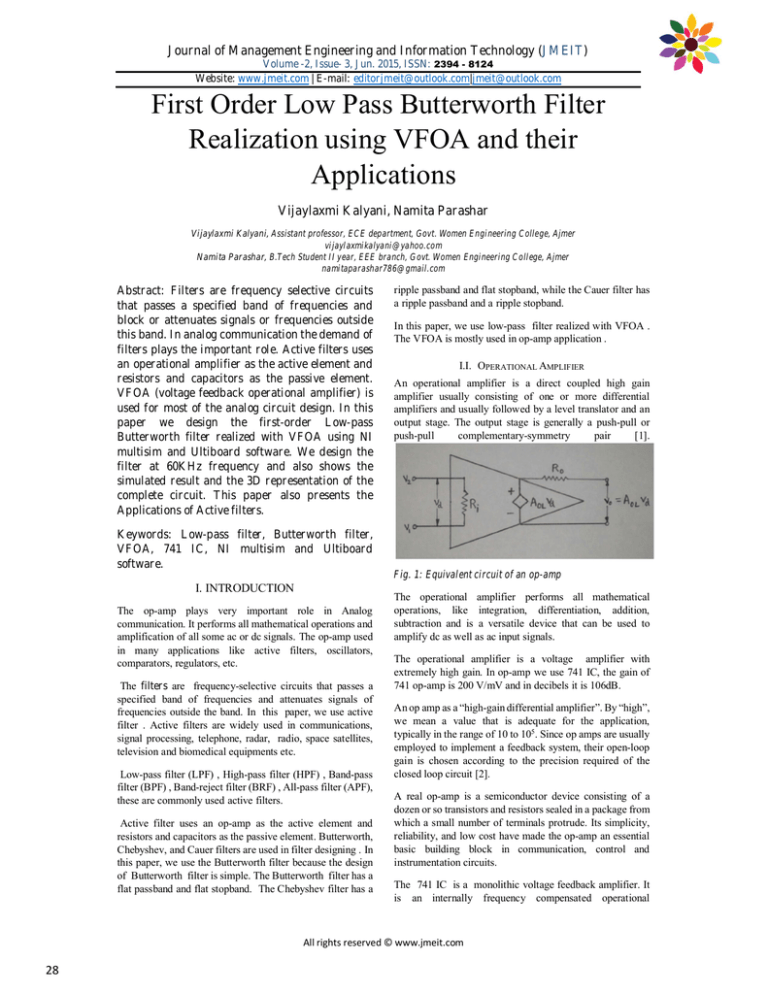
An operational amplifier is a direct coupled high gain
amplifier usually consisting of one or more differential
amplifiers and usually followed by a level translator and an
output stage. The output stage is generally a push-pull or
push-pull
complementary-symmetry
pair
[1].
Keywords: Low-pass filter, Butterworth filter,
VFOA, 741 IC, NI multisim and Ultiboard
software.
Fig. 1: Equivalent circuit of an op-amp
I. INTRODUCTION
The op-amp plays very important role in Analog
communication. It performs all mathematical operations and
amplification of all some ac or dc signals. The op-amp used
in many applications like active filters, oscillators,
comparators, regulators, etc.
The filters are frequency-selective circuits that passes a
specified band of frequencies and attenuates signals of
frequencies outside the band. In this paper, we use active
filter . Active filters are widely used in communications,
signal processing, telephone, radar, radio, space satellites,
television and biomedical equipments etc.
Low-pass filter (LPF) , High-pass filter (HPF) , Band-pass
filter (BPF) , Band-reject filter (BRF) , All-pass filter (APF),
these are commonly used active filters.
Active filter uses an op-amp as the active element and
resistors and capacitors as the passive element. Butterworth,
Chebyshev, and Cauer filters are used in filter designing . In
this paper, we use the Butterworth filter because the design
of Butterworth filter is simple. The Butterworth filter has a
flat passband and flat stopband. The Chebyshev filter has a
The operational amplifier performs all mathematical
operations, like integration, differentiation, addition,
subtraction and is a versatile device that can be used to
amplify dc as well as ac input signals.
The operational amplifier is a voltage amplifier with
extremely high gain. In op-amp we use 741 IC, the gain of
741 op-amp is 200 V/mV and in decibels it is 106dB.
An op amp as a “high-gain differential amplifier”. By “high”,
we mean a value that is adequate for the application,
typically in the range of 10 to 105. Since op amps are usually
employed to implement a feedback system, their open-loop
gain is chosen according to the precision required of the
closed loop circuit [2].
A real op-amp is a semiconductor device consisting of a
dozen or so transistors and resistors sealed in a package from
which a small number of terminals protrude. Its simplicity,
reliability, and low cost have made the op-amp an essential
basic building block in communication, control and
instrumentation circuits.
The 741 IC is a monolithic voltage feedback amplifier. It
is an internally frequency compensated operational
All rights reserved © www.jmeit.com
28
Journal of Management Engineering and Information Technology (JMEIT)
Volume -2, Issue- 3, Jun. 2015, ISSN: 2394 - 8124
Website: www.jmeit.com | E-mail: editorjmeit@outlook.com|jmeit@outlook.com
The gain magnitude and phase angle equations of lowamplifier. It has absolute rating of supply voltage as ±22V ,
pass filter can be obtained by converting Equation (2) into its
slew rate 0.5V/µsec, settling time 0.3µsec and overshoot
equivalent polar form, as follows:
45%. It has high gain, wide range of operating voltage
compensation network (6dB/octave) ensuring stability in
|v0/vin| = Af/√1+(f/fH)2
(3)
closed loop circuit [3].
I.II. VOLTAGE FEEDBACK OPERATIONAL AMPLIFIER (VFOA)
VFOA is widely used in all analog circuit design. VFOA is
mostly used in op-amp application. VFOA have been with
us for about 60 years and in VFOA the feedback that makes
them versatile and accurate also has a tendency to make them
unstable. The operational amplifier circuit configuration
uses a high gain amplifier whose parameters are determined
by external feedback components. The amplifier gain is so
high that without these external feedback components, the
slightest input signal would saturate the amplifier output [3].
In many applications like realization of voltage controlled
current sources (VCCS), instrumentation amplifiers, noninverting integrators and non-inverting differentiators etc.
where the traditional VFOA based circuits suffer from
problems like employment of more than the required no. of
passive components, their perfect matching required because
their mismatch may lead to instability, gain bandwidth
conflict, slew rate distortion due to finite slew rate.
II. FIRST-ORDER LOW-PASS BUTTERWORTH FILTER
The low-pass filter selects particular band of frequency, i.e.
it passes low frequencies and stop high frequencies. This
filter uses an RC network for filtering and the Op-amp is
used in the non-inverting configuration; hence it does not
load down the RC network. Resistors R1 and Rf determine
the gain of the filter. According to the voltage-divider rule,
the voltage at the non-inverting terminal (across capacitor C)
is
v1 = (-jXc/R-jXc).vin
Phase angle in degrees = – tan-1 (f/f H)
(4)
The operation of the Low-Pass Filter can be verified from the
gain magnitude equation, (3):
1. At very low frequencies, that is, f < f H
|v0/vin| = Af
2. At f = fH
|v0vin| = Af /√2 = 0.707Af
3. At f >fH
|v0 /vin | < Af
The rate at which the gain rolls off after fH is 20 dB/decade.
III. LOW PASS FILTER DESIGNING STEPS
A low pass filter can be designed by implementing the
following steps:
1. Choose the value of high cut-off frequency f.
2. Select the value of C i.e. (C ≤ 1µf)
3. Calculate the value of R using R= 1/2πfHC
4. Select the value of R1 and Rf dependent on the desired
passband gain using Af = 1 + Rf/R1
Thus we select the component according to the designing
steps. We design the low pass filter with a cut-off frequency
of 60 KHz
(1)
where
Thus f H = fC = 60 KHz
j = (-1)1/2 and –jXc = 1/j2 fC
Let C = .05 µf, Thus R = .053 KΩ and R1 = 10 KΩ, R2=8KΩ
Simplifying equation (1), we get
IV. DESIGN AND SIMULATION OF LOW PASS FILTER
USING 741IC
v1 = vin/(1+j2πfRC)
and the output voltage
VEE
-15V
v0 = {1 + (Rf/R1)}.v1
XSC1
That is,
XBP1
Ext Trig
+
_
R2
v0 = {1+(Rf/R1)}.vin/(1+j2πfRC)
XFG1
_
+
OUT
_
U1
4
OR
IN
B
A
+
8kΩ
R1
2
10kΩ
v0/vin = Af /{1+j(f/fH)}
(2)
6
3
7 1 5
where
C1
.05µF
v0/vin = gain of the filter as a function of frequency
f = frequency of the input signal
15V
Fig. 2: circuit diagram of low pass filter using NI multisim
fH = 1/ (2πRC) = high cutoff frequency of the filter
All rights reserved © www.jmeit.com
29
R4
10kΩ
VCC
R5
.053kΩ 50%
Key=A
Af = 1 + Rf/R1 = passband gain of the filter
741
Journal of Management Engineering and Information Technology (JMEIT)
Volume -2, Issue- 3, Jun. 2015, ISSN: 2394 - 8124
Website: www.jmeit.com | E-mail: editorjmeit@outlook.com|jmeit@outlook.com
Fig.6: 3-D view of low pass filter
Fig.3: output waveform of low pass filter up to 3000 KHz
X. V. APPLICATIONS
•
•
•
•
•
•
Fig.4: frequency response of low pass filter using Bode
Plotter
Due to its maximum flat pass band response it is
used as anti-aliasing filter in data converter
applications.
It has applications in radars such as in designing
the display of radar target track.
These are used in quality audio applications.
These are used in digital filters for motion
analysis.
Low-pass filter is used to stabilize amplifiers by
rolling off the gain at higher frequencies where
excessive phase shift may cause oscillations.
Filters can be used to separate signals, passing
those of interest, and attenuating the unwanted
frequencies.
. VI. RESULT
We design the first order low pass Butterworth filter at
frequency of 60 KHz. The output waveform obtained up to
3000 KHz. After simulation the gain is obtained approx. 2.6
dB at 51.438 KHz using bode plotter.
VII. CONCLUSION AND FUTURE WORK
Fig.5: Ultiboard design of low pass filter
In this paper, we designed the first order low pass
Butterworth filter at 60 KHz. The low pass Butterworth filter
are maximally flat as an amplitude response in the passband,
and there is no ripple in passband. We also used the
Ultiboard for the design and 3-D view is also shown. VFOA
is mostly used in op-amp application but the capacitive
compensation of VFOA limits their slew rate, finite gain
bandwidth product destabilizes the circuit at high
frequencies, so here we can also use the CFOA (current
feedback operational amplifier). CFOAs have ideally infinite
slew rate. In practice, slew rates from several hundred V/µs
to as high as 9,000 V/µs are attainable. A CFOA-based
circuit would operate satisfactorily over a frequency range
much larger than possible for a VFOA circuit realizing the
same function.
All rights reserved © www.jmeit.com
30
Journal of Management Engineering and Information Technology (JMEIT)
Volume -2, Issue- 3, Jun. 2015, ISSN: 2394 - 8124
Website: www.jmeit.com | E-mail: editorjmeit@outlook.com|jmeit@outlook.com
Journals, National Journals and Conferences, MemberREFERENCES
IAENG.
[1] Ramakant A. Gayakwad, “Op-amps and Linear Integrated
Circuits,”
fourth
ed.,
2005.
[2] Behzad Razavi, “Design of Analog CMOS Integrated Circuits.”
[3] Vijaylaxmi Kalyani, Aayushi Arya, “Design and Simulation of
VFA and CFA Based Integrator and Differentiator using NI
Multisim and their Comparison,” IJARECE vol. 3, no.8, August
2014.
Namita Parashar is pursuing her B.Tech. (II-year) in
Electrical and Electronics Engineering in GWEC, Ajmer.
She is Coordinator and member of ISTE.
AUTHOR’S DETAIL
VijayLaxmi Kalyani is currently working as Assistant
Professor in the department of ECE in GWEC, Ajmer. She
has attended various workshops, conferences, FDP, STC and
also published many research papers in Various International
All rights reserved © www.jmeit.com
31
