ACPL-M71T and ACPL-M72T
High Speed, Low Power Digital Optocouplers
with R2Coupler™ Isolation and AEC-Q100 Grade 1 Qualification
Data Sheet
Description
Features
The Avago ACPL-M71T and ACPL-M72T are high temperature, digital CMOS optocouplers in SOIC-5 packages.
Suitable for hybrid and electric vehicle applications,
the optocouplers use the latest CMOS IC technology to
achieve outstanding performance and very low power
consumption. All devices are AEC-Q100 compliant and
operate over the –40°C to 125 °C temperature range.
• 5 V CMOS compatible
The ACPL-M71T uses a high speed LED, and the ACPL-M72T
uses a low current LED for lower power dissipation. The
high speed ACPL-M71T featuring a 35 ns maximum
propagation delay (IF =10 mA). The ACPL-M72T optocoupler features very low power. With a low 4 mA LED drive
current, ACPL-M72T typical propagation delay is 60 ns.
Each digital optocoupler has a CMOS detector IC, an integrated photodiode, a high speed transimpedance
amplifier, and a voltage comparator with an output
driver.
Avago R2Coupler isolation products provide the reinforced insulation and reliability needed for critical in automotive and high temperature industrial applications
• Common-Mode Rejection 40kV/µs @ VCM=1000V:
• Wide automotive temperature range: –40°C to 125°C
• Low propagation delay :
– High Speed ACPL-M71T: 26ns @ IF = 10 mA (Typical)
– Low Power ACPL-M72T: 60ns @ IF = 4 mA (Typical)
• Worldwide safety approval:
– UL 1577 recognized, 4000 Vrms / 1 min
– CSA approved
– IEC/EN/DIN EN 60747-5-5
• Qualified to AEC-Q100 Grade 1 test guidelines
Applications
• Automotive CANBus communications interface
• Automotive isolated high speed gate drivers for IGBTs
and Power MOSFETs
• High temperature digital signal isolation
• Microcontroller interface
• Digital isolation for A/D and D/A conversion
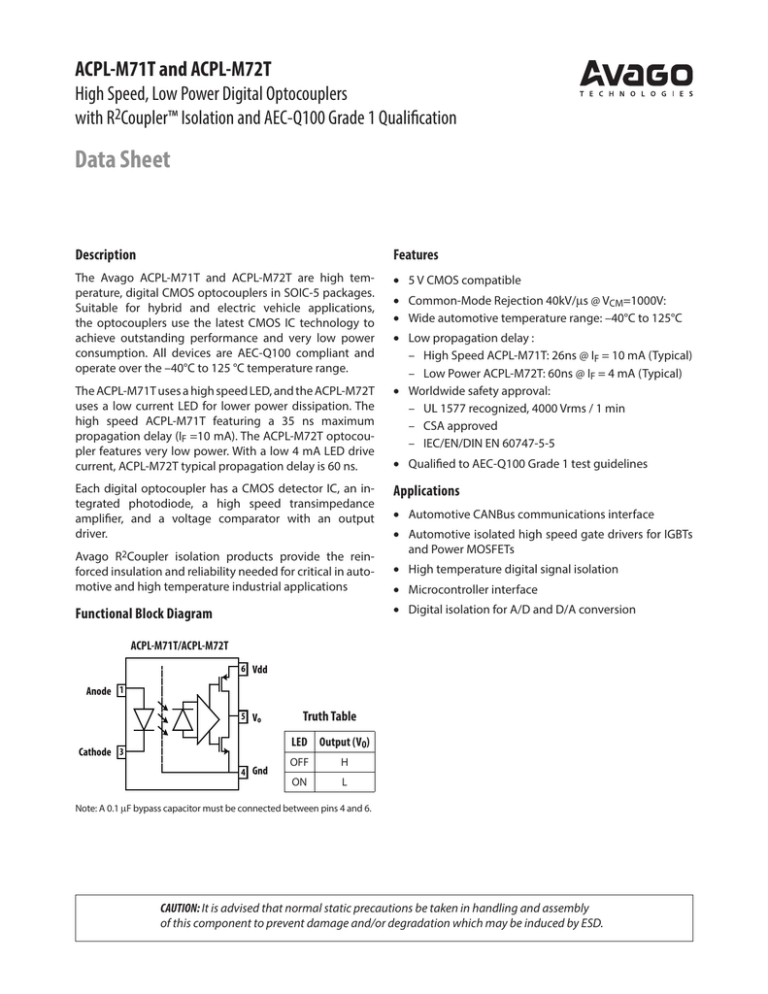
Functional Block Diagram
ACPL-M71T/ACPL-M72T
6 Vdd
Anode 1
5 Vo
Truth Table
LED Output (VO)
Cathode 3
4 Gnd
OFF
H
ON
L
Note: A 0.1 µF bypass capacitor must be connected between pins 4 and 6.
CAUTION: It is advised that normal static precautions be taken in handling and assembly
of this component to prevent damage and/or degradation which may be induced by ESD.
Ordering Information
Option
Part Number
(RoHS) Compliant
Package
Surface Mount
ACPL-M71T
-000E
SO-5
X
ACPL-M72T
X
-500E
X
X
-560E
X
X
SO-5
Quantity
100 per tube
-060E
-000E
IEC/EN/DIN EN
60747-5-5
Tape & Reel
X
100 per tube
1500 per reel
X
1500 per reel
X
100 per tube
-060E
X
-500E
X
X
X
-560E
X
X
100 per tube
1500 per reel
X
1500 per reel
To order, choose a part number from the part number column and combine with the desired option from the option
column to form an order entry.
For example, the part number ACPL-M71T-500E describes a device with a surface mount SOIC-5 package; delivered in
Tape and Reel with 1500 parts per reel; and full RoHS compliance.
Option datasheets are available. Contact your Avago sales representative or authorized distributor for information.
Package Dimensions
ACPL-M71T / ACPL-M72T (JEDEC MO-155 Package)
ANODE 1
M71T
YWW
EE
4.4 ± 0.1
(0.173 ± 0.004)
7.0 ± 0.2
(0.276 ± 0.008)
CATHODE 3
0.4 ± 0.05
(0.016 ± 0.002)
6
V CC
5
V OUT
4
GND
Extended Datecode
for lot tracking
3.6 ± 0.1*
(0.142 ± 0.004)
2.5 ± 0.1
(0.098 ± 0.004)
0.102 ± 0.102
(0.004 ± 0.004)
0.20 ± 0.025
(0.008 ± 0.001)
7° MAX.
1.27 BSC
(0.050)
DIMENSIONS IN MILLIMETERS (INCHES)
* MAXIMUM MOLD FLASH ON EACH SIDE IS 0.15 mm (0.006)
NOTE: FLOATING LEAD PROTRUSION IS 0.15 mm (6 mils) MAX.
2
0.71 MIN
(0.028)
MAX. LEAD COPLANARITY
= 0.102 (0.004)
Land Pattern Recommendation
4.4
(0.17)
1.3
(0.05)
2.5
(0.10)
2.0
(0.080)
0.64
(0.025)
8.27
(0.325)
DIMENSION IN MILLIMETERS (INCHES)
Recommended Pb-Free IR Profile
Recommended reflow condition as per JEDEC Standard, J-STD-020 (latest revision).
Note: Non-halide flux should be used.
Regulatory Information
The ACPL-M71T and ACPL-M72T are approved by the following organizations:
UL
IEC/EN/DIN EN 60747-5-5
Approved under UL 1577, component recognition
program up to VISO = 4000 VRMS.
IEC 60747-5-5:
EN 60747-5-5:
DIN EN 60747-5-5:
CSA
Approved under CSA Component Acceptance Notice #5.
3
Insulation and Safety Related Specifications
Parameter
Symbol
Value
Units
Conditions
Minimum External Air
Gap (Clearance)
L(I01)
>5
mm
Measured from input terminals to output terminals,
shortest distance through air.
Minimum External
Tracking (Creepage)
L(I02)
>5
mm
Measured from input terminals to output terminals,
shortest distance path along body.
0.08
mm
Insulation thickness between emitter and detector;
also known as distance through insulation.
>175
V
DIN IEC 112/VDE 0303 Part 1
Minimum Internal Plastic
Gap (Internal Clearance)
Tracking Resistance
(Comparative Tracking Index)
CTI
Isolation Group
IIIa
Material Group (DIN VDE 0109)
IEC/EN/DIN EN 60747-5-5 Insulation Related Characteristics
Description
Symbol
ACPL-M71T/
ACPL-M72T
Units
Maximum Working Insulation Voltage
VIORM
567
VPEAK
Input to Output Test Voltage, Method b†
VPR
1063
VPEAK
Input to Output Test Voltage, Method a†
VIORM x 1.6 = VPR, Type and Sample Test,
tm = 10 sec, Partial Discharge < 5 pC
VPR
907
VPEAK
Highest Allowable Overvoltage†
(Transient Overvoltage, tini = 60 sec)
VIOTM
6000
VPEAK
Case Temperature
Ts
150
°C
Input Current
Is, INPUT
150
mA
Output Power
Ps,OUTPUT
600
mW
Insulation Resistance at TS, VIO = 500 V
RIO
≥109
Ω
VIORM x 1.875 = VPR, 100% Production
Test with tm = 1 sec, Partial Discharge < 5 pC
Safety Limiting Values
(Maximum values allowed in the event of a failure,
also see Thermal Derating curve, Figure 11.)
4
Absolute Maximum Ratings
Parameter
Symbol
Min.
Max.
Units
Storage Temperature
TS
–55
+130
°C
Ambient Operating Temperature[1]
TA
–40
+125
°C
Supply Voltages
VDD
0
6.5
V
Output Voltage
VO
–0.5
VDD +0.5
V
Average Forward Input Current
IF
–
20.0
mA
Peak Transient Input Current
(IF at 1 µs pulse width, <10% duty cycle)
IF( TRAN)
1
80
A
mA
Reverse Input Voltage
Vr
5
V
Input Power Dissipation
PI
40
mW
Output Power Dissipation
Po
30
mW
–
Condition
<1 µs Pulse Width, 300 pps
<1 µs Pulse Width,
<10%Duty Cycle
Lead Solder Temperature
260 °C for 10 sec., 1.6 mm below seating plane
Solder Reflow Temperature Profile
See Solder Reflow Temperature Profile Section
Recommended Operating Conditions
Parameter
Symbol
Min.
Max.
Units
Ambient Operating Temperature
TA
–40
+125
°C
Supply Voltages
VDD
3.0
5.5
V
Forward Input Current
IF(ON)
4.0
15
mA
Forward Off State Voltage
VF (OFF)
0.8
V
Input Threshold Current
ITH
3.5
mA
5
Electrical Specifications
Over recommended temperature (TA = –40°C to +125°C), 3.0 V ≤VDD ≤ 5.5 V. All typical specifications are at TA=+25°C,
VDD= +5V.
Parameter
Symbol
Min.
Typ.
Max.
Input Capacitance
CIN
Input Reverse
Breakdown Voltage
BVR
5.0
V
IR = 10 µA
Logic High Output Voltage
VOH
VDD-0.6
V
IOH = -4mA
4
Logic Low Output Voltage
VOL
0.6
V
IOL = 4mA
3
Logic Low Output Supply
Current
IDDL
0.9
1.5
mA
Logic High Output Supply
Current
IDDH
0.9
1.5
mA
LED Forward Voltage
Vf
1.45
1.5
1.75
V
IF=10mA, Ta=25°C
1.25
1.5
1.85
V
IF=10mA, Ta= -40°C ~ 125°C
90
Vf Temperature Coeficient
Units
Test Conditions
Fig
pF
-1.5
mV/°C
ACPL-M71T High Speed Mode Switching Specifications
Over recommended temperature (TA = –40°C to +125°C), 4.5 V ≤VDD ≤ 5.5 V. All typical specifications are at TA=+25°C,
VDD = 5V.
Parameter
Symbol
Propagation Delay Time to
Logic Low Output[1]
Typ.
Max.
Units
Test Conditions
Fig
Note
tPHL
26
35
ns
5,6,11
1,2,3
Propagation Delay Time to
Logic High Output[1]
tPLH
26
35
ns
Vin=4.5V-5.5V,
Rin=390Ω+/-5%, Cin=100pF,
CL= 15pF
Pulse Width Distortion[2]
PWD
0
12
ns
Propagation Delay Skew[3]
tPSK
15
ns
Output Rise Time
(10% – 90%)
tR
10
ns
Output Fall Time
(90% - 10%)
tF
10
ns
Common Mode Transient
Immunity at Logic High
Output[4]
| CMH |
15
25
kV/µs
Vin=0V Rin=390Ω +/-5%,
Cin=100pF, Vcm=1000V,
TA=25°C
12
4
Common Mode Transient
Immunity at Logic High
Output[5]
| CML |
15
25
kV/µs
Vin=4.5V-5.5V ,
Rin=390Ω +/-5%, Cin=100pF,
Vcm=1000V, TA=25°C
13
5
6
Min.
ACPL-M72T Low Power Mode Switching Specifications
Over recommended temperature (-40°C to +125°C), 3.0V ≤ VDD ≤ 5.5V. All typical specifications at +25°C and VDD = 5V
Parameter
Symbol
Propagation Delay Time to
Logic Low Output[1]
Min.
Typ.
Max.
Units
Test Conditions
Fig
Note
tPHL
60
100
ns
IF=4mA, CL=15pF
1,2,3
Propagation Delay Time to
Logic High Output[1]
tPLH
35
100
ns
7,8,
9,10,
14
Pulse Width Distortion[2]
PWD
25
50
ns
Propagation Delay Skew[3]
tPSK
60
ns
Output Rise Time
(10% – 90%)
tR
10
ns
Output Fall Time
(90% - 10%)
tF
10
ns
Common Mode Transient
Immunity at Logic High
Output[4]
| CMH |
25
40
kV/µs
Using Avago LED Driving
Circuit,
VIN=0V, R1=350Ω+/-5% ,
R2=350Ω+/-5%, VCM=1000V,
TA=25°C
15
4
Common Mode Transient
Immunity at Logic High
Output[5]
| CML |
25
40
kV/µs
Using Avago LED Driving
Circuit,
VIN=4.5-5.5V, R1=350Ω+/-5% ,
R2=350Ω, VCM=1000V, TA=25°C
16
5
Package Characteristics
All Typical at TA = 25°C.
Parameter
Symbol
Min.
Input-Output Momentary
Withstand Voltage
VISO
4000
Input-Output Resistance
R I-O
Input-Output Capacitance
C I-O
Typ.
Max.
Units
Test Conditions
Vrms
RH ≤ 50%, t = 1 min.,
TA = 25°C
1014
Ω
VI-O = 500 V dc
0.6
pF
f = 1 MHz, TA = 25°C
Notes:
1.tPHL propagation delay is measured from the 50% (Vin or If ) on the rising edge of the input pulse to 0.8V on the falling edge of the VO signal. tPLH
propagation delay is measured from the 50% (Vin or If ) on the falling edge of the input pulse to the 80% level of the rising edge of the VO signal.
2. PWD is defined as |tPHL - tPLH|.
3. tPSK is equal to the magnitude of the worst case difference in tPHL and/or tPLH that will be seen between units at any given temperature within the
recommended operating conditions.
4. CMH is the maximum tolerable rate of rise of the common mode voltage to assure that the output will remain in a high logic state.
5. CML is the maximum tolerable rate of fall of the common mode voltage to assure that the output will remain in a low logic state.
7
Performance Plots
100.00
5
10.00
Vo - Output Voltage (V)
IF - Forward Current (mA)
Ta = 25°C
1.00
0.10
0.01
1.2
1.3
1.4
1.5
VF - Forward Voltage - V
VOH - Logic High Output Voltage - V
VOL - Logic Low Output Voltage - V
0.600
0.500
0.400
0.300
0.200
0.100
0
0.5
2
0
2
4
6
8
IOL - Logic Low Output Current - mA
10
4.6
4.4
4.2
4.0
0
40
35
35
30
25
20
TPHL Vin=4.5V, Rin=390Ω, Cin=100pF
TPLH
PWD
15
10
5
-40
-20
0
20 40 60 80
Temperature - °C
100
120
-2
-4
-6
-8
IOH - Logic High Output Current - mA
-10
Figure 4. Typical Logic High Output Voltage vs Logic High Output Current
40
0
1
1.5
IF - Forward Current - mA
4.8
Tp - Propagation Delay, PWD - Pulse
Width Distortion - ns
Tp - Propagation Delay, PWD - Pulse
Width Distortion - ns
1
5.0
Figure 3. Typical Logic Low Output Voltage vs Logic Low Output Current
140
Figure 5. ACPL-M71T (High Speed)Typical Propagation Delay vs Temperature
8
2
Figure 2. Typical Output Voltage vs Input Forward Current
0.700
0.000
3
0
1.6
Figure 1. Typical Diode Input Forward Current Characteristic
4
30
25
20
15
TPHL Rin=390Ω, Cin=100pF
TPLH Ta=25°C
PWD
10
5
0
-5
3
4
5
6
7 8 9 10 11 12 13 14 15
IF - Forward Current - mA
Figure 6. ACPL-M71T (High Speed)Typical Propagation Delay vs Forward
Current - IF
TPHL IF=4mA
TPLH
PWD
-20
0
20
40
60
80
Temperature - °C
100
60
55
50
45
40
35
30
25
20
15
10
5
0
-5
-10
120
Figure 7. ACPL-M72T (5V) Typical Propagation Delay vs Temperature
5
6
7 8 9 10 11 12 13 14 15
IF - Forward Current - mA
50
40
30
20
-20
0
20
40
60
80
TA - Temperature - °C
TA = 25 ° C, V DD =3V
70
TP - Propagation Delay - ns
TP - Propagation Delay - ns
60
T PHL
T PLH
PWD
10
100
Figure 9. ACPL-M72T (3V) Typical Propagation Delay vs Temperature
9
4
80
IF = 4mA, VDD =3V
70
0
-40
3
Figure 8. ACPL-M72T (5V) Typical Propagation Delay vs Forward Current - IF
90
80
TPHL
TPLH Ta=25°C
PWD
Tp - Propagation Delay, PWD - Pulse
Width Distortion - ns
Width Distortion - ns
50
45
40
35
30
25
20
15
10
5
0
-5
-40
120
60
50
T PHL
T PLH
PWD
40
30
20
10
0
3
4
5
6
7 8 9 10 11 12 13 14 15
IF - Forward Current - mA
Figure 10. ACPL-M72T (3V) Typical Propagation Delay vs Input Forward
Current
Test Circuit Diagrams
ACPL-M71T High Speed Mode:
Vdd=5 V
ACPL-M71T
Cin=100pF
Vin
6
R1=390±5%
Vin=4.5 - 5.5 V
0
0.1 µF
Bypass Cap
1
Vdd
VO
5
CL=15pF
3
GND1
OUTPUT Vo
MONITORING
NODE
80% Vdd
4
SHIELD
Vin
2
Vin
2
0.8 V
VOL
GND2
tPHL
tPLH
Figure 11. High Speed Mode Test Circuit and Typical Waveform
Vdd=5 V
Cin=100pF
ACPL-M71T
6
0.1 µF
Bypass Cap
1
R1=390±5%
CL=15pF
3
Vin=4.5 - 5.5 V
OUTPUT Vo
MONITORING
NODE
4
SHIELD
V CM (PEAK)
VCM
5
0V
VO
5V
SWITCH AT A: I F = 0 mA
V dd-1
CM H
GND2
GND2
+
−
High Voltage Pulse
VCM = 1000V
Figure 12. High Speed Mode CMH Test Circuit and Typical Waveform
Vdd=5 V
Cin=100pF
ACPL-M71T
6
0.1 µF
Bypass Cap
1
R1=390±5%
5
CL=15pF
Vin=4.5 - 5.5 V
3
4
SHIELD
GND2
+
−
High Voltage Pulse
VCM = 1000V
Figure 13. High Speed Mode CML Test Circuit and Typical Waveform
10
VCM
OUTPUT Vo
MONITORING
NODE
V CM (PEAK)
0V
VO
GND2
SWITCH AT A: I F = 0 mA
1V
CM L
ACPL-M72T Low Power Mode:
Vdd=5 V
ACPL-M72T
Vin
6
PULSE GEN.
0
0.1 µF
Bypass Cap
1
OUTPUT Vo
MONITORING
NODE
CL=15pF
3
0.8 V
tPHL
Figure 14. Low Power Mode Switching Test Circuit and Typical Waveform
Vdd=5 V
ACPL-M72T
R1=350
6
0.1 µF
Bypass Cap
1
5
CL=15pF
R2=350
3
OUTPUT Vo
MONITORING
NODE
4
SHIELD
GND2
+
−
High Voltage Pulse
VCM = 1000V
Figure 15. Low Power Mode High CMR, CMH Test Circuit
Vdd=5 V
ACPL-M72T
R1=350
6
0.1 µF
Bypass Cap
1
5
CL=15pF
R2=350
3
4
SHIELD
GND2
+
−
High Voltage Pulse
VCM = 1000V
Figure 16. Low Power Mode High CMR, CML Test Circuit
11
VOL
GND2
GND1
Vin =
4.5 - 5.5V
80% Vdd
4
SHIELD
Rin=700
Vdd
VO
5
INPUT
MONITORING
NODE
Vin
2
Vin
2
OUTPUT Vo
MONITORING
NODE
tPLH
Application Circuits
LOGIC I/O
Ro
Cin
Vdd
Vin
Truth Table
RLIMIT
Vout
0.1 µF
Bypass Cap
GND1
Vin
LED
Vout
L
ON
L
H
OFF
H
SHIELD
GND2
Figure 17. Recommended Application Circuit for ACPL-M71T High Speed Performance
LOGIC I/O
Ro
Vin
Vdd
½RLIMIT
Truth Table
Vout
½RLIMIT
GND1
0.1 µF
Bypass Cap
Vin
LED
Vout
L
ON
L
H
OFF
H
SHIELD
GND2
Figure 18. Recommended Application Circuit for ACPL-M72T Low Power Performance
For product information and a complete list of distributors, please go to our web site:
www.avagotech.com
Avago, Avago Technologies, the A logo and R2Coupler™ are trademarks of Avago Technologies in the United States and other countries.
Data subject to change. Copyright © 2005-2014 Avago Technologies. All rights reserved.
AV02-2180EN - June 30, 2014


