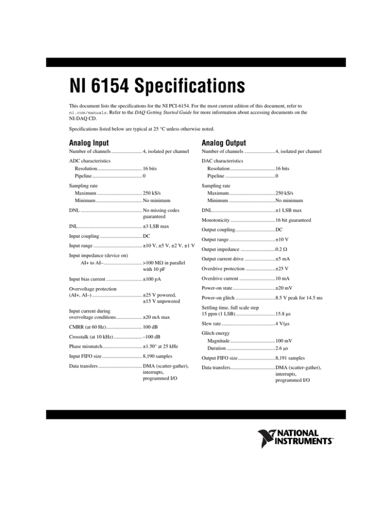
NI 6154 Specifications
This document lists the specifications for the NI PCI-6154. For the most current edition of this document, refer to
ni.com/manuals. Refer to the DAQ Getting Started Guide for more information about accessing documents on the
NI-DAQ CD.
Specifications listed below are typical at 25 °C unless otherwise noted.
Analog Input
Analog Output
Number of channels ........................ 4, isolated per channel
Number of channels ........................4, isolated per channel
ADC characteristics
Resolution................................... 16 bits
Pipeline....................................... 0
DAC characteristics
Resolution ...................................16 bits
Pipeline .......................................0
Sampling rate
Maximum ................................... 250 kS/s
Minimum .................................... No minimum
Sampling rate
Maximum....................................250 kS/s
Minimum ....................................No minimum
DNL ................................................ No missing codes
guaranteed
DNL.................................................±1 LSB max
INL.................................................. ±3 LSB max
Input coupling ................................. DC
Input range ...................................... ±10 V, ±5 V, ±2 V, ±1 V
Input impedance (device on)
AI+ to AI–.............................. >100 MΩ in parallel
with 10 pF
Monotonicity ...................................16 bit guaranteed
Output coupling...............................DC
Output range ....................................±10 V
Output impedance ...........................0.2 Ω
Output current drive ........................±5 mA
Overdrive protection .......................±25 V
Input bias current ............................ ±100 pA
Overdrive current ............................10 mA
Overvoltage protection
(AI+, AI–) ....................................... ±25 V powered,
±15 V unpowered
Power-on state .................................±20 mV
Input current during
overvoltage conditions .................... ±20 mA max
CMRR (at 60 Hz)............................ 100 dB
Power-on glitch ...............................8.5 V peak for 14.5 ms
Settling time, full scale step
15 ppm (1 LSB)...............................15.8 μs
Slew rate ..........................................4 V/μs
Phase mismatch............................... ±1.50° at 25 kHz
Glitch energy
Magnitude ...................................100 mV
Duration ......................................2.6 μs
Input FIFO size ............................... 8,190 samples
Output FIFO size .............................8,191 samples
Data transfers .................................. DMA (scatter-gather),
interrupts,
programmed I/O
Data transfers...................................DMA (scatter-gather),
interrupts,
programmed I/O
Crosstalk (at 10 kHz) ...................... –100 dB
Table 1. NI 6154 Analog Input Range-Dependent Characteristics
1 –3
2
Input Range
Bandwidth1
(kHz)
THD
(dB at 10 kHz)
System Noise
(LSBrms)
SFDR Typ2
(dB)
±10 V
275
–85
0.9
95
±5 V
270
–85
1.2
95
±2 V
158
–90
1.7
90
±1 V
132
–85
2.3
85
dB frequency
Measured at 100 kHz, not including harmonics.
Typical Performance Graphs
Analog Input CMRR with
Respect to Earth Ground
Grounded Input Power Spectrum,
(250 kS/s, 8,192 points)
0
120
10 V Range
110
–40
CMRR (dB)
Magnitude (dB)
–20
–60
–80
–100
–120
100 5 V Range
2 V Range
90
1 V Range
80
70
–140
0
20
40
60
80
Frequency (kHz)
100
60
0.01
120
0.1
1.0
Frequency (kHz)
10
100
Normalized Signal Amplitude (dB)
Analog Input Bandwidth
5
0
–5
10 V Range
–10
5 V Range
–15
–20
0.1
2 V Range
1 V Range
1.0
NI 6154 Specifications
10
100
Frequency (kHz)
1000
2
ni.com
© National Instruments Corporation
3
NI 6154 Specifications
–10
–5
–2
–1
10
5
2
1
194
194
194
194
Residual
Gain Error
(ppm of
Reading)
156
156
162
112
Gain
Tempco
(ppm/°C)
5
5
5
5
Reference
Tempco
150
120
90
60
Residual
Offset
Error
(ppm of
Range)
23
17
13
12
Offset
Tempco
(ppm of
Range/°C)
92
92
92
92
INL Error
(ppm of
Range)
71
103
188
262
Random
Noise, σ
(μVrms)
686
1,289
3,061
5,279
Absolute
Accuracy
at Full
Scale1 (μV)
Sensitivity is the smallest voltage change that can be detected. It is a function of noise.
AbsoluteAccuracy = 10 V · (GainError) + 10 V · (OffsetError) + NoiseUncertainty AbsoluteAccuracy = 5,279 μV
For example, on the 10 V range, the absolute accuracy at full scale is as follows:
GainError = 194 ppm + 112 ppm · 1 + 5 ppm · 10
GainError = 356 ppm
OffsetError = 60 ppm + 12 ppm · 1 + 92 ppm
OffsetError = 164 ppm
262 μV ⋅ 3NoiseUncertainty = ------------------------NoiseUncertainty = 79 μV
100
Absolute accuracy at full scale on the analog input channels is determined using the following assumptions:
TempChangeFromLastExternalCal = 10 °C
TempChangeFromLastInternalCal = 1 °C
number_of_readings = 100
CoverageFactor = 3 σ
Accuracies listed are valid for up to one year from the device external calibration.
2
1
AbsoluteAccuracy = Reading · (GainError) + Range · (OffsetError) + NoiseUncertainty
GainError = ResidualAIGainError + GainTempco · (TempChangeFromLastInternalCal) + ReferenceTempco · (TempChangeFromLastExternalCal)
OffsetError = ResidualAIOffsetError + OffsetTempco · (TempChangeFromLastInternalCal) + INL_Error
RandomNoise ⋅ 3
NoiseUncertainty = ----------------------------------------For a coverage factor of 3 σ and averaging 100 points.
100
Negative
Full Scale
Positive
Full Scale
Nominal Range
AI Absolute Accuracy Table
28
41
75
105
Sensitivity2
(μV)
NI 6154 Specifications
4
ni.com
–10
10
209
Residual Gain
Error (ppm of
Reading)
105
Gain Tempco
(ppm/°C)
5
Reference
Tempco
80
Residual
Offset Error
(ppm of
Range)
111
Offset Tempco
(ppm of
Range/°C)
244
INL Error
(ppm of
Range)
7,991
Absolute
Accuracy at
Full Scale1
(μV)
AbsoluteAccuracy = OutputValue · (GainError) + Range · (OffsetError)
GainError = ResidualGainError + GainTempco · (TempChangeFromLastInternalCal) + ReferenceTempco · (TempChangeFromLastExternalCal)
OffsetError = ResidualOffsetError + AOOffsetTempco · (TempChangeFromLastInternalCal) + INL_Error
1 Absolute Accuracy at full scale numbers is valid immediately following internal calibration and assumes the device is operating within 10 °C of the last external calibration.
Accuracies listed are valid for up to one year from the device external calibration.
Negative
Full Scale
Positive
Full Scale
Nominal Range
AO Absolute Accuracy Table
Digital I/O
Phase-Locked Loop (PLL)
Number of channels ........................ 6 DI PFI <0..5>,
4 DO PFI <6..9>
Direction control ............................. None, each terminal
has a fixed direction
Number of PLLs..............................1
Reference signal ..............................RTSI <0..7>
Output of PLL .................................80 MHz timebase; other
signals derived from
80 MHz timebase
including 20 MHz and
100 kHz timebases.
Compatibility .................................. 5 V TTL
Functionality ................................... Static digital input,
static digital output,
timing input,
timing output
External Digital Trigger
Input voltage protection .................. ±20 V on up to two pins
Source..............................................PFI <0..5> or RTSI
Recommended Operating Conditions
Polarity ............................................Software-selectable
Level
RTSI Trigger Lines
Min
Max
VIH input high voltage
2.0 V
5.25 V
VIL input low voltage
0V
0.8 V
IOH output high current (VOH = 4.0 V)
—
–6 mA
Bus Interface
IOH output high current (VOH = 2.8 V)
—
–24 mA
PCI...................................................3.3 V or 5 V signaling
IOL output low current (VOL = 0.4 V)
—
7 mA
IOL output low current (VOL = 1.4 V)
—
24 mA
Trigger lines <0..6>.........................7
RTSI clock.......................................1
Power Requirements
+5 V.................................................1.3 A
General Purpose Counter/Timers
Physical
Number of counter/timers ............... 2
Dimensions......................................15.6 cm × 9.8 cm
(6.2 in. × 3.9 in.)
Resolution ....................................... 32 bits
Weight .............................................198 g (7.0 oz)
Internal base clocks......................... 80 MHz, 20 MHz,
100 kHz
I/O connector...................................1 37-pin D-SUB
External base clock frequency ........ 0 Hz to 20 MHz
Environmental
Base clock accuracy........................ 50 ppm
Operating temperature.....................0 to 50 °C
FIFO................................................ 2 samples
Storage temperature.........................–20 to 70 °C
Data transfers .................................. DMA, interrupts,
programmed I/O
Humidity..........................................5 to 95% RH,
noncondensing
Frequency Generator
Maximum altitude ...........................2,000 m
Number of channels ........................ 1
Pollution Degree
(indoor use only) .............................2
Base clocks ..................................... 10 MHz, 100 kHz
Divisors ........................................... 1 to 16
Calibration (AI and AO)
Base clock accuracy........................ 50 ppm
Recommended warm-up time .........15 minutes
Calibration interval..........................1 year
© National Instruments Corporation
5
NI 6154 Specifications
Maximum Working Voltage1
Figure 1 illustrates the maximum working voltage
specifications.
Channel-to-channel2
Continuous ..................................≤30 Vrms/60 VDC,
Measurement Category I3
Va
AI+ x/AO+ x
Vb
AI– x/AO– x
Vc
AI+ y/AO+ y
Continuous ..................................≤30 Vrms/60 VDC,
Measurement Category I3
Vd
AI– y/AO– y
Withstand ....................................≤840 Vrms/1,200 VDC,
verified by a 5 s dielectric
withstand test
Ve
PFI x
Vf
D GND
Withstand ....................................≤840 Vrms/1,200 VDC,
verified by a 5 s dielectric
withstand test
Channel-to-earth ground4
PCI-Bus
Backplane
Bus
Isolation Barrier
Channel-to-bus5
Vg
Continuous ..................................≤30 Vrms/60 VDC,
Measurement Category I3
Vh
Withstand ....................................≤1,400 Vrms/
1,950 VDC, verified by a
5 s dielectric withstand
test
Figure 1. NI 6154 Maximum Working Voltage
AI+ to AI–
(in Figure 1, ⎪Va – Vb⎪) ..................≤11 V, Measurement
Category I3
Safety
This product is designed to meet the requirements of the
following standards of safety for electrical equipment for
measurement, control, and laboratory use:
PFI x to D GND
(in Figure 1, ⎪Ve – Vf ⎪)...................≤5.25 V, Measurement
Category I3
Caution This device is rated for Measurement
Category I and the voltage across the isolation
barrier is limited to no greater than
30 Vrms/60 VDC/42.4 Vpk. Do not use for
measurements within Categories II, III, or IV.
1
2
3
4
5
•
IEC 61010-1, EN 61010-1
•
UL 61010-1, CAN/CSA-C22.2 No. 61010-1
Note For UL and other safety certifications,
refer to the product label, or visit ni.com/
certification, search by model number or
product line, and click the appropriate link in the
Certification column.
Maximum working voltage refers to the signal voltage plus the common-mode voltage.
In Figure 1, ⎪Va,Vb – Vc,Vd⎪, ⎪Va,Vb – Ve,Vf⎪, and ⎪Vc,Vd – Ve,Vf⎪.
Measurement Category I is for measurements performed on circuits not directly connected to the electrical distribution system
referred to as MAINS voltage. MAINS is a hazardous live electrical supply system that powers equipment. This category is
for measurements of voltages from specially protected secondary circuits. Such voltage measurements include signal levels,
special equipment, limited-energy parts of equipment, circuits powered by regulated low-voltage sources, and electronics.
In Figure 1, ⎪Va – Vh⎪, ⎪Vb – Vh⎪, ⎪Vc – Vh⎪, ⎪Vd – Vh⎪, ⎪Ve – Vh⎪, and ⎪Vf – Vh⎪.
In Figure 1, ⎪Va – Vg⎪, ⎪Vb – Vg⎪, ⎪Vc – Vg⎪, ⎪Vd – Vg⎪, ⎪Ve – Vg⎪, and ⎪Vf – Vg⎪.
NI 6154 Specifications
6
ni.com
Electromagnetic Compatibility
This product is designed to meet the requirements of the
following standards of EMC for electrical equipment for
measurement, control, and laboratory use:
•
EN 61326 EMC requirements; Minimum Immunity
AI 0+
•
EN 55011 Emissions; Group 1, Class A
•
CE, C-Tick, ICES, and FCC Part 15 Emissions; Class A
AI 1–
NC
AI 2+
Notes For EMC compliance, operate this device
with shielded cabling.
Please refer to the S Series Help for EMC cabling
issues.
CE Compliance
This product meets the essential requirements of applicable
European Directives, as amended for CE marking, as follows:
•
73/23/EEC; Low-Voltage Directive (safety)
•
89/336/EEC; Electromagnetic Compatibility
Directive (EMC)
AI 3–
NC
AO 0+
AO 1–
NC
AO 2+
AO 3–
NC
PFI 1/P0.1
PFI 2/P0.2
PFI 4/P0.4
Note Refer to the Declaration of Conformity
(DoC) for this product for any additional regulatory
compliance information. To obtain the DoC for
this product, visit ni.com/certification, search
by model number or product line, and click the
appropriate link in the Certification column.
PFI 5/P0.5
PFI 7/P1.1
PFI 8/P1.2
20
21
22
23
24
25
26
27
28
29
30
31
32
33
34
35
36
37
1
2
3
4
5
6
7
8
9
10
11
12
13
14
15
16
17
18
19
AI 0–
NC
AI 1+
AI 2–
NC
AI 3+
AO 0–
NC
AO 1+
AO 2–
NC
AO 3+
PFI 0/P0.0
D GND
PFI 3/P0.3
D GND
PFI 6/P1.0
D GND
PFI 9/P1.3
NC = No Connect
Waste Electrical and Electronic
Equipment (WEEE)
EU Customers At the end of their life cycle, all
products must be sent to a WEEE recycling center.
For more information about WEEE recycling
centers and National Instruments WEEE initiatives,
visit ni.com/environment/weee.htm.
Figure 2. NI 6154 Pinout
National Instruments, NI, ni.com, and LabVIEW are trademarks of National Instruments Corporation.
Refer to the Terms of Use section on ni.com/legal for more information about National
Instruments trademarks. Other product and company names mentioned herein are trademarks or trade
names of their respective companies. For patents covering National Instruments products, refer to the
appropriate location: Help»Patents in your software, the patents.txt file on your CD, or
ni.com/patents.
© 2006 National Instruments Corporation. All rights reserved.
371669C-01
Jul06
