Freescale Semiconductor
Application Note
AN3456
Rev 0, 04/2007
Generating a Supply Rail for the MC34940
and MC33941 in Low Voltage Systems
This application note demonstrates how to generate the
supply voltage required by Freescale’s MC34940 and
MC33941 Electric Field Imaging Devices in low voltage
systems that do not have an appropriate voltage available.
Inductive boost and regulated charge pump techniques are
compared and example circuits are given using off-the-shelf
components.
The MC34940/33941 is an Electric Field Imaging Device
used in cost-sensitive applications where non-contact sensing
of objects is desired. The MC34940 generates a typically
120 kHz, low distortion sine wave, which is detected on its
seven electrode inputs that are connected to external sense
electrodes. Changes in external electrical conductance on the
external electrodes are measured by the MC34940/33941.
Common applications for the MC34940/33941 are user
interface touch panels and liquid presence and level
detection.
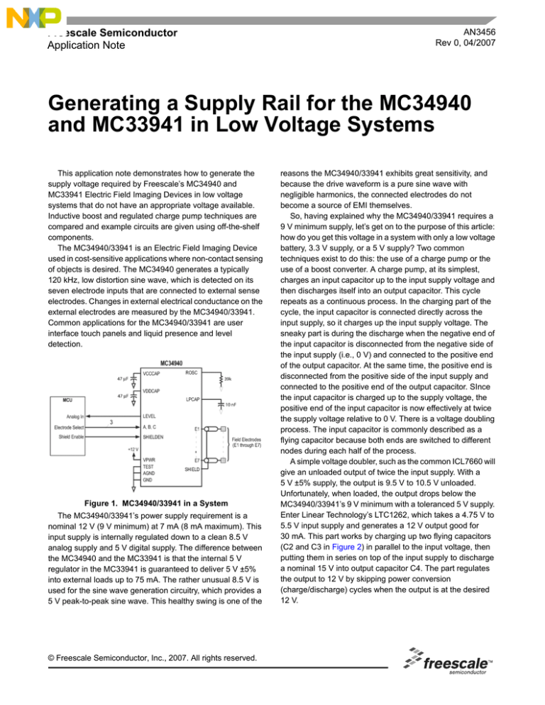
Figure 1. MC34940/33941 in a System
The MC34940/33941’s power supply requirement is a
nominal 12 V (9 V minimum) at 7 mA (8 mA maximum). This
input supply is internally regulated down to a clean 8.5 V
analog supply and 5 V digital supply. The difference between
the MC34940 and the MC33941 is that the internal 5 V
regulator in the MC33941 is guaranteed to deliver 5 V ±5%
into external loads up to 75 mA. The rather unusual 8.5 V is
used for the sine wave generation circuitry, which provides a
5 V peak-to-peak sine wave. This healthy swing is one of the
© Freescale Semiconductor, Inc., 2007. All rights reserved.
reasons the MC34940/33941 exhibits great sensitivity, and
because the drive waveform is a pure sine wave with
negligible harmonics, the connected electrodes do not
become a source of EMI themselves.
So, having explained why the MC34940/33941 requires a
9 V minimum supply, let’s get on to the purpose of this article:
how do you get this voltage in a system with only a low voltage
battery, 3.3 V supply, or a 5 V supply? Two common
techniques exist to do this: the use of a charge pump or the
use of a boost converter. A charge pump, at its simplest,
charges an input capacitor up to the input supply voltage and
then discharges itself into an output capacitor. This cycle
repeats as a continuous process. In the charging part of the
cycle, the input capacitor is connected directly across the
input supply, so it charges up the input supply voltage. The
sneaky part is during the discharge when the negative end of
the input capacitor is disconnected from the negative side of
the input supply (i.e., 0 V) and connected to the positive end
of the output capacitor. At the same time, the positive end is
disconnected from the positive side of the input supply and
connected to the positive end of the output capacitor. SInce
the input capacitor is charged up to the supply voltage, the
positive end of the input capacitor is now effectively at twice
the supply voltage relative to 0 V. There is a voltage doubling
process. The input capacitor is commonly described as a
flying capacitor because both ends are switched to different
nodes during each half of the process.
A simple voltage doubler, such as the common ICL7660 will
give an unloaded output of twice the input supply. With a
5 V ±5% supply, the output is 9.5 V to 10.5 V unloaded.
Unfortunately, when loaded, the output drops below the
MC34940/33941’s 9 V minimum with a toleranced 5 V supply.
Enter Linear Technology’s LTC1262, which takes a 4.75 V to
5.5 V input supply and generates a 12 V output good for
30 mA. This part works by charging up two flying capacitors
(C2 and C3 in Figure 2) in parallel to the input voltage, then
putting them in series on top of the input supply to discharge
a nominal 15 V into output capacitor C4. The part regulates
the output to 12 V by skipping power conversion
(charge/discharge) cycles when the output is at the desired
12 V.
POWERING EXTERNAL CIRCUITS FROM THE
MC34940/33941’S +5 V OUTPUT
Figure 2. LTC1262 Charge Pump
The LTC1262 is a good solution for systems with a 5 V
supply, but what about lower voltage systems? Here we have
to turn to boost converters with an inductor. Boost converters
work by ramping up current from the input supply through an
inductor and power switch to ground, then turning off the
switch. An output diode steers the inductor current to an
output capacitor where the energy is stored as the cycle
repeats. There are many suitable low cost boost converters
that can be used, and the trick is to pick one that is not rated
at an unnecessarily higher output than is needed. Picking a
boost converter that is just good enough means that the
inductor, diode, and capacitor peak current ratings are low and
cheap. The ON Semiconductor NCP1403SNT1, shown in
Figure 3, happily delivers the MC34940/33941’s worst-case
requirement of 8 mA from an input voltage of below 2 V. This
circuit is suitable for 2-cell, 3-cell and single Li-ION powered
applications, as well as from nominal 3 V and 5 V rails. The
NCP1403SNT1 comes in a small SOT23-5 package as does
the BAR43C dual-diode. The capacitors can be surface mount
ceramic and the TDK sourced inductor is only 4.8 mm long by
3.4 mm wide.
The circuit in Figure 3 regulates its output at a nominal
9.7 V which is set by resistors R1 and R2. This is comfortably
above the 9 V minimum required by the MC34940/33941, but
not unnecessarily high to waste system power. The output
voltage with an 8 mA load on the prototype varied from 9.8 V
with a 5 V input supply down to 9.57 V with input down at 2 V.
The MC34940/33941’s internal 5 V regulator will also
supply 5 V into external loads up to 75 mA. This regulated
output may be useful in low voltage systems (powered by
sources such as dual AA cells, or a single Li-ION cell) which
needs 5 V for other parts of the system. Simple boost
converters with internal current limits, such as the
NCP1402SNT1, have reducing output current capability as
input voltage reduces. This is shown in Figure 4. This means
that the available extra current from the MC34940/33941’s 5 V
output is dependent on your minimum supply voltage to the
NCP1402SNT1. For example, a Li-ION battery with a 3 V
minimum voltage will allow you to draw 24 mA from the
MC34940/33941’s 5 V output
Figure 4. NCP1403SNT1 Output Current vs. Input Voltage
Figure 3. NCP1403SNT1 Boost Converter
AN3456
2
Sensors
Freescale Semiconductor
How to Reach Us:
Home Page:
www.freescale.com
Web Support:
http://www.freescale.com/support
USA/Europe or Locations Not Listed:
Freescale Semiconductor, Inc.
Technical Information Center, EL516
2100 East Elliot Road
Tempe, Arizona 85284
+1-800-521-6274 or +1-480-768-2130
www.freescale.com/support
Europe, Middle East, and Africa:
Freescale Halbleiter Deutschland GmbH
Technical Information Center
Schatzbogen 7
81829 Muenchen, Germany
+44 1296 380 456 (English)
+46 8 52200080 (English)
+49 89 92103 559 (German)
+33 1 69 35 48 48 (French)
www.freescale.com/support
Japan:
Freescale Semiconductor Japan Ltd.
Headquarters
ARCO Tower 15F
1-8-1, Shimo-Meguro, Meguro-ku,
Tokyo 153-0064
Japan
0120 191014 or +81 3 5437 9125
support.japan@freescale.com
Asia/Pacific:
Freescale Semiconductor Hong Kong Ltd.
Technical Information Center
2 Dai King Street
Tai Po Industrial Estate
Tai Po, N.T., Hong Kong
+800 2666 8080
support.asia@freescale.com
For Literature Requests Only:
Freescale Semiconductor Literature Distribution Center
P.O. Box 5405
Denver, Colorado 80217
1-800-441-2447 or 303-675-2140
Fax: 303-675-2150
LDCForFreescaleSemiconductor@hibbertgroup.com
AN3456
Rev. 0
04/2007
Information in this document is provided solely to enable system and software
implementers to use Freescale Semiconductor products. There are no express or
implied copyright licenses granted hereunder to design or fabricate any integrated
circuits or integrated circuits based on the information in this document.
Freescale Semiconductor reserves the right to make changes without further notice to
any products herein. Freescale Semiconductor makes no warranty, representation or
guarantee regarding the suitability of its products for any particular purpose, nor does
Freescale Semiconductor assume any liability arising out of the application or use of any
product or circuit, and specifically disclaims any and all liability, including without
limitation consequential or incidental damages. “Typical” parameters that may be
provided in Freescale Semiconductor data sheets and/or specifications can and do vary
in different applications and actual performance may vary over time. All operating
parameters, including “Typicals”, must be validated for each customer application by
customer’s technical experts. Freescale Semiconductor does not convey any license
under its patent rights nor the rights of others. Freescale Semiconductor products are
not designed, intended, or authorized for use as components in systems intended for
surgical implant into the body, or other applications intended to support or sustain life,
or for any other application in which the failure of the Freescale Semiconductor product
could create a situation where personal injury or death may occur. Should Buyer
purchase or use Freescale Semiconductor products for any such unintended or
unauthorized application, Buyer shall indemnify and hold Freescale Semiconductor and
its officers, employees, subsidiaries, affiliates, and distributors harmless against all
claims, costs, damages, and expenses, and reasonable attorney fees arising out of,
directly or indirectly, any claim of personal injury or death associated with such
unintended or unauthorized use, even if such claim alleges that Freescale
Semiconductor was negligent regarding the design or manufacture of the part.
Freescale™ and the Freescale logo are trademarks of Freescale Semiconductor, Inc.
All other product or service names are the property of their respective owners.
© Freescale Semiconductor, Inc. 2007. All rights reserved.
