Microelectronic Engineering 88 (2011) 2691–2693
Contents lists available at ScienceDirect
Microelectronic Engineering
journal homepage: www.elsevier.com/locate/mee
Processing of 50 nm gate-length hydrogen terminated diamond FETs for high
frequency and high power applications
D.A.J. Moran a,⇑, D.A. MacLaren b, S. Porro c, H. McLelland a, P. John c, J.I.B. Wilson c
a
Electronics and Electrical Engineering, University of Glasgow, Glasgow G12 8LT, UK
Physics and Astronomy, University of Glasgow, Glasgow G12 8QQ, UK
c
Engineering and Physical Sciences, Heriot-Watt University, Edinburgh EH14 4AS, UK
b
a r t i c l e
i n f o
Article history:
Received 19 September 2010
Accepted 17 November 2010
Available online 23 November 2010
Keywords:
Diamond
FET
Hydrogen-terminated
50 nm
a b s t r a c t
To better understand the intrinsic scaling limitations of sub-100 nm gate-length hydrogen-terminated
diamond Field Effect Transistors (FETs), the fabrication and DC characterisation of 50 nm gate length
devices have been investigated. Physical processing of the hydrogenated diamond surface presents a
challenge for the realisation of short gate length, high performance devices due to the inherent sensitivity
of the surface to device processing. Through the development of a finely optimised device fabrication process, we have demonstrated transistor operation at a reduced gate length of 50 nm. This is believed to be
the shortest gate length operational diamond transistor yet reported. Inspection of device operation at
larger voltages indicates the onset of potential short channel effects, attributed to the reduced dimensions of the gate. This is an important result in the investigation of the high frequency and high power
potential of hydrogen terminated diamond transistors.
Ó 2010 Elsevier B.V. All rights reserved.
1. Introduction
Many of the unique and extreme physical properties of the diamond material system deem it an ideal active material for high
power/high frequency transistor development. Such properties include a large bandgap for high voltage operation (5.5 eV) [1], high
intrinsic electron and hole mobility related to high frequency performance (3800–4500 cm2/V s) [2], and the largest thermal conductivity of any solid, allowing for efficient heat diffusion during
high power operation (22 W/K cm) [1]. At present, charge carrier
densities attainable at room temperature and suitable for high
power device operation can be achieved in diamond by either boron doping during material growth, or by hydrogen terminating the
surface. Both result in p-type conductivity, with the latter forming
a 2-dimensional hole layer approximately 5–10 nm below the diamond surface in the presence of select surface adsorbates [3]. The
hydrogen terminated diamond surface has demonstrated excellent
potential in the development of high power/high frequency transistors for gate lengths around 100 nm [4,5]. However, the typical
fabrication process for these devices relies on the direct formation
of ohmic contacts by wet chemical etching of a surface gold protective layer, minimizing exposure of the sensitive hydrogenated diamond surface to processing [6]. Large contact line-edge roughness
and a symmetric gate to ohmic contact separation are inherent to
⇑ Corresponding author.
E-mail address: d.moran@elec.gla.ac.uk (D.A.J. Moran).
0167-9317/$ - see front matter Ó 2010 Elsevier B.V. All rights reserved.
doi:10.1016/j.mee.2010.11.029
this process as shown in Fig. 1, both of which are highly undesirable for the realisation of aggressively scaled power devices.
We report on the implementation of a fabrication process in
contrast to that in [4], which uses an additional ohmic contact
lithography stage to minimise ohmic contact edge roughness,
and allows for asymmetric positioning of the gate between the
source and drain contacts. The DC operation of 50 nm devices fabricated by this process is then discussed.
2. Method
CVD grown 10 10 mm (0 1 1)-orientated polycrystalline diamond was supplied by Element 6. Samples were hydrogen terminated using a hot filament process forming a surface 2D hole gas
with carrier concentration 9e12 cm 2 and mobility of 70 cm2/V s
as verified by Van Der Pauw measurement. 50 nm gate length
FET devices were fabricated using the process flow presented in
Fig. 2: all lithographical stages of the device process were patterned using PMMA resist and a Vistec VB6 electron beam lithography tool operating at 100 keV. Initially a gold protection layer
is deposited by electron beam evaporation directly onto the hydrogenated diamond surface. The gold is then removed outwith device
active areas by potassium iodide based wet etching, using PMMA
as an etch mask. Treatment of the exposed diamond surface to oxygen plasma ensures removal of the hydrogen termination in unmasked regions and allows for electrical isolation of individual
devices. Following definition of the 50 nm gate resist profile, the
2692
D.A.J. Moran et al. / Microelectronic Engineering 88 (2011) 2691–2693
Fig. 3. Transmission Electron Microscope (TEM) device cross section confirming
50 nm gate dimension and asymmetric gate positioning towards the source contact.
Fig. 1. Directly etched gold ohmic contact FET device structure demonstrating
contact edge roughness and inherent symmetric gate alignment.
Fig. 4. Device output (Id vs. Vds for fixed Vgs) response.
Fig. 2. Fifty nanometer FET device fabrication process flow.
gold layer is wet etched back, allowing for metallisation and lift-off
of the aluminium gate metal onto the diamond surface. This stage
marks the device completion of the publicised process of [4],
whereby the remaining gold protective layer to either side of the
gate forms the ohmic contacts (Fig. 1). To guarantee minimal ohmic contact edge roughness and provide positional control of the
gate relative to the source and drain contacts, we perform an additional ohmic contact level after gate formation as part of our device
process. Following resist patterning of this additional layer, the
remaining gold on the diamond surface is removed by wet etch
to allow for deposition and lift-off of a ‘fresh’ gold ohmic metallisation directly onto the diamond. An undesirable consequence of
performing this additional lithography step is a substantial
increase in the device access resistance. This is attributed to
increased ohmic contact resistance where gold ohmic metal is redeposited onto the previously exposed diamond surface after etching of the original gold at the gate level. In regions where gold still
protects the surface before being etched and re-deposited, very little increase in ohmic contact resistance is observed. Similarly, the
sheet resistance of the exposed diamond between the gate and ohmic contacts was not observed to degrade as a consequence of the
final ohmic lithography level. Ensuring minimal increase in access
resistance utilising this device process therefore relies on minimising the overlapping contact area of re-deposited gold onto the pre-
viously exposed diamond surface. Although this can be achieved by
reducing the lateral distance of the gold etch at the gate level, the
large line-edge roughness of the gold makes it difficult to completely eliminate such overlap without substantially large gate to
ohmic contact separation. However, fine optimisation of the gold
etch process at gate level has led to the realisation of substantial
performance 50 nm gate length FETs.
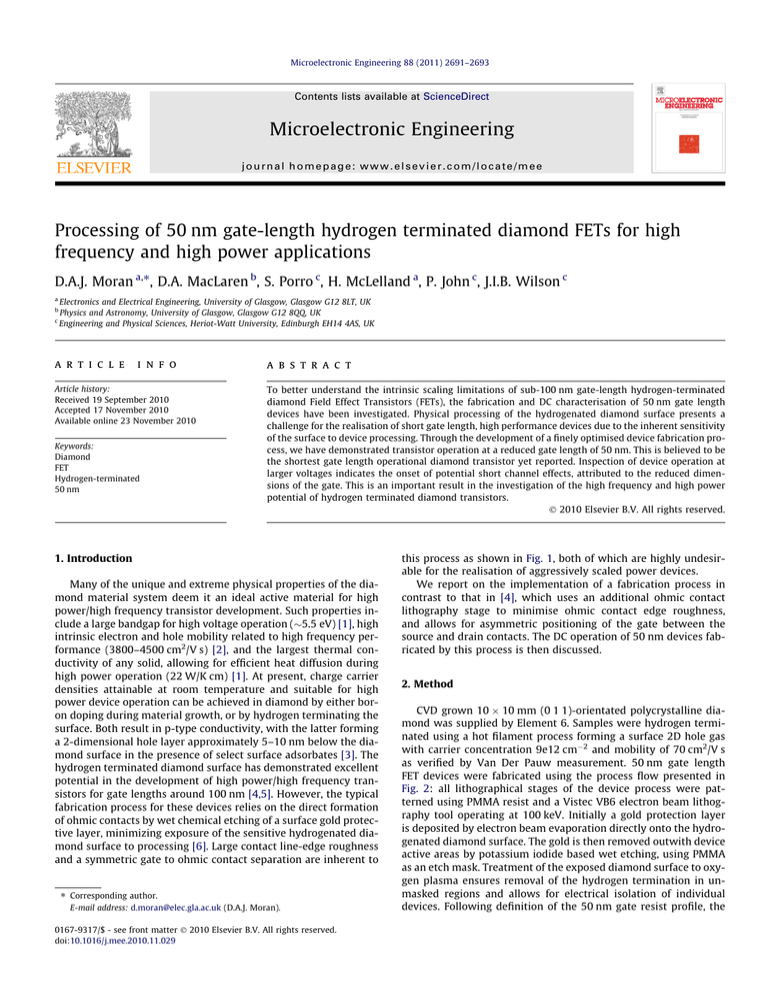
A Transmission Electron Microscope (TEM) image of a completed 50 nm device is shown in Fig. 3. An asymmetric device
geometry is adopted whereby the gate is positioned closer to the
source contact than the drain contact. This acts to reduce electric
field strength towards the drain side of the gate and increase onstate power operation.
3. Results and discussion
Completed 50 nm gate length devices were 50 lm in width, of a
single gate finger layout and were designed specifically for DC
characterisation. Device DC output characteristics are shown in
Fig. 4. Where a maximum drain current approaching 80 mA/mm
is observed at a source–drain bias of 10 V Vds. A peak extrinsic
transconductance of 12 mS/mm is also extracted for these devices.
It should be noted that transmission line model (TLM) test structures fabricated on the same sample and using directly etched gold
ohmic contacts typically achieved saturation currents in excess of
500 mA/mm. This suggests degradation of the device saturation
current which can be attributed to an increase in access resistance
due to the formation of the device ohmic contacts by the additional
ohmic lithography level. Such an increase in parasitic resistance
will not affect the intrinsic scaling behaviour of the device however, the investigation of which is the prime focus of this work.
Inspection of the gate control characteristics in Fig. 4 indicate that
under lower bias, efficient transistor operation can be maintained
D.A.J. Moran et al. / Microelectronic Engineering 88 (2011) 2691–2693
2693
source–drain bias. This phenomenon cannot be attributed to gate
leakage current, which as is demonstrated in Fig. 6, remains minimal across this bias range. Instead, the observed increase in the offstate output conductance and sub-threshold swing is most likely
indicative of ‘short channel effects’, suggesting that for a 50 nm
gate geometry, we are approaching the intrinsic limit whereby
we can produce an efficient, high performance device.
4. Conclusions
Fig. 5. Logarithmic device transfer (Id vs. Vgs for fixed Vds) response.
Fifty nanometer gate-length hydrogen terminated diamond
FETs have been fabricated using a finely optimised etch and ohmic
re-deposition process. By defining the ohmic contacts using an
additional lithography level, contact edge roughness is greatly reduced and accurate positioning of the gate contact relative to the
source and drain can be achieved. Completed device performance
suggests parasitic access resistance is increased as a side effect of
adopting this process. Independent of access resistance however,
the intrinsic device operation is observed from device DC characteristics and demonstrates efficient transistor operation and pinch
off of the drain current is achieved at lower source–drain bias. Increased off-state output conductance under higher bias operation
indicates most likely the onset of short channel effects, attributable
to the reduced dimensions of the gate contact. Further optimisation to processing and device geometry should yield improved performance and greater understanding of operation of sub-100 nm
hydrogenated diamond FETs.
Acknowledgements
This work was supported by EPSRC project EP/E054668/1. The
authors would like to thank Element 6 and Diamond Microwave
Devices for material supply and their support of the research.
References
Fig. 6. Device gate leakage current (Ig vs. Vgs for fixed Vds) characteristics.
and the drain current ‘pinched off’. At more positive gate and more
negative drain bias however, electrostatic control of the underlying
hole current by the 50 nm gate becomes less efficient and an increase in the output conductance occurs at approximately 7 V
Vds. This is more readily observed upon inspection of the device
logarithmic transfer characteristics in Fig. 5 where the sub-threshold swing is found to increase substantially with more negative
[1] B. Ozpineci, L.M. Tolbert, S.K. Islam, M. Chinthavali, in: European Conference on
Power Electronics and Applications, Toulouse, France, 2003.
[2] J. Isberg, J. Hammersberg, E. Johansson, T. Wikström, D. Twitchen, A.J.
Whitehead, S.E. Coe, G.A. Scarsbrook, Science 297 (5587) (2002) 1670–1672.
[3] F. Maier, M. Riedel, B. Mantel, J. Ristein, L. Ley, Physical Review Letters 85 (16)
(2000) 3472–3475.
[4] K. Ueda, M. Kasu, Y. Yamauchi, T. Makimoto, M. Schwitters, D.J. Twitchen, G.A.
Scarsbrook, S.E. Coe, IEEE Electron Device Letters 27 (7) (2006) 570–572.
[5] K. Hirama, H. Takayanagi, S. Yamauchi, Y. Jingu, H. Umezawa, H. Kawarada, in:
IEEE Electron Devices Meeting, Washington, DC, USA, 2007, pp. 873–876.
[6] M. Kubovic, A. Aleksov, A. Denisenko, E. Kohn, in: IEEE Lester Eastman
Conference on High Performance Devices, Newark, USA, 2002, pp. 90–99.


