ISSN 2321-8665
Vol.03,Issue.04,
July-2015,
Pages:0640-0645
WWW.IJITECH.ORG
Power Factor Improvement using Single-Stage Balanced Forward
Flyback Converter
MADISHETTY VENKATESH KUMAR1, K. CHANDRA MOULI2
1
PG Scholar, Vaageswari College of Engineering, Ramakrishna Colony, Karimnagar, Telangana, India.
Assoc Prof, Vaageswari College of Engineering, Ramakrishna Colony, Karimnagar, Telangana, India.
2
Abstract: In this paper, a high efficiency and high power
factor single-stage balanced forward-flyback converter
merging a foward and flyback converter topologies is
proposed. The conventional AC/DC flyback converter can
achieve a good power factor but it has a high offset current
through the transformer magnetizing inductor, which results
in a large core loss and low power conversion efficiency.
And, the conventional forward converter can achieve the
good power conversion efficiency with the aid of the low
core loss but the input current dead zone near zero cross AC
input voltage deteriorates the power factor. On the other
hand, since the proposed converter can operate as the forward
and flyback converters during switch on and off periods,
respectively, it cannot only perform the power transfer during
an entire switching period but also achieve the high power
factor due to the flyback operation. Moreover, since the
current balanced capacitor can minimize the offset current
through the transformer magnetizing inductor regardless of
the AC input voltage, the core loss and volume of the
transformer can be minimized. Therefore, the proposed
converter features a high efficiency and high power factor. To
confirm the validity of the proposed converter, theoretical
analysis and experimental resultsfrom a prototype of 24W
LED driver are presented.
factor corrector and isolated DC/DC converter). The first
stage provides a near unity power factor and low total
harmonic distortion (THD) over an entire range of universal
inputvoltage (90-270 Vrms) and the second DC/DC stage is
used to provide a tight output regulation and galvanic
isolation between AC input and DC output. Even though the
two-stage configuration can provide the high power factor,
good output regulation and excellent ripple voltage, it has
several significant disadvantages such as a large system size,
high cost of production and low energy conversion efficiency.
Therefore, it is common that the two-stage driver is mainly
used for high power applications and single-stage driver is
adopted as a low power LED driver.
Keywords: Conventional AC/DC, Flyback Converter.
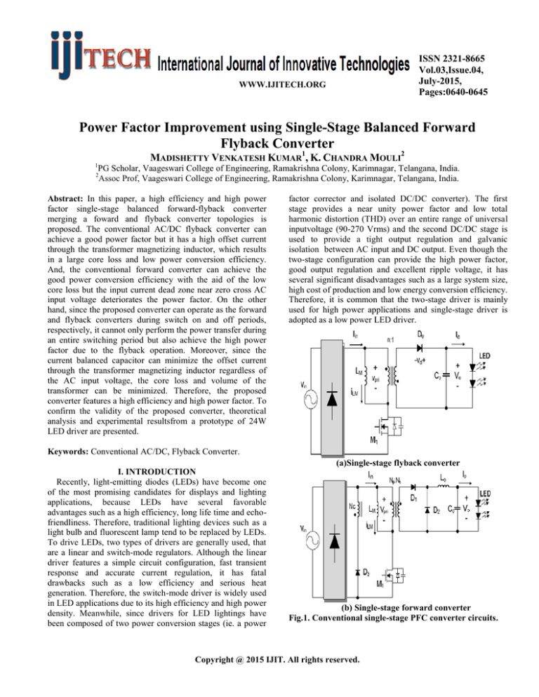
(a)Single-stage flyback converter
I. INTRODUCTION
Recently, light-emitting diodes (LEDs) have become one
of the most promising candidates for displays and lighting
applications, because LEDs have several favorable
advantages such as a high efficiency, long life time and echofriendliness. Therefore, traditional lighting devices such as a
light bulb and fluorescent lamp tend to be replaced by LEDs.
To drive LEDs, two types of drivers are generally used, that
are a linear and switch-mode regulators. Although the linear
driver features a simple circuit configuration, fast transient
response and accurate current regulation, it has fatal
drawbacks such as a low efficiency and serious heat
generation. Therefore, the switch-mode driver is widely used
in LED applications due to its high efficiency and high power
density. Meanwhile, since drivers for LED lightings have
been composed of two power conversion stages (ie. a power
(b) Single-stage forward converter
Fig.1. Conventional single-stage PFC converter circuits.
Copyright @ 2015 IJIT. All rights reserved.
MADISHETTY VENKATESH KUMAR, K. CHANDRA MOULI
Fig.1(a) shows conventional single-stage PFC (power
Fig.2 shows the basic topology of a fly-back circuit. Input
factor correction) LED drivers, which are well known as most
to the circuit may be unregulated dc voltage derived from the
cost effective solutions. Fig1(b) shows their transformer
utility ac supply after rectification and some filtering. The
magnetizing inductor currents. As shown in this figure, the
ripple in dc voltage waveform is generally of low frequency
magnetizing inductor offset current of flyback converter is
and the overall ripple voltage waveform repeats at twice the
larger than that of forward converter as followings
ac mains frequency. Since the SMPS circuit is operated at
much higher frequency (in the range of 100 kHz) the input
voltage, in spite of being unregulated, may be considered to
(1)
have a constant magnitude during any high frequency cycle.
A fast switching device („S‟), like a MOSFET, is used with
fast dynamic control over switch duty ratio (ratio of ON time
to switching time-period) to maintain the desired output
(2)
voltage. The transformer, in Fig.2, is used for voltage
Moreover, from equations(1) and (2), while the magnetizing
isolation as well as for better matching between input and
inductor offset current of flyback converter is dependent on
output voltage and current requirements.
the load current Io, that of forward converter is not.
Therefore, as the load current is more increased, the offset
III. AC –DC CONVERTER
current of flyback converter becomes larger, which might
A. Introduction
result in the larger core loss and volume of transformer. For
A rectifier is an electrical device that converts alternating
these reasons, the forward converter is superior to the flyback
current (AC), which periodically reverses direction, to direct
converter in terms of the transformer size and energy
current (DC), which flows in only one direction. The process
conversion efficiency.
is known as rectification. Physically, rectifiers take a number
of forms, including vacuum tube diodes, mercury-arc valves,
II. FLY BACK CONVERTER
copper and selenium oxide rectifiers, semiconductor diodes,
A. Introduction
silicon-controlled rectifiers and other silicon-based
Fly-back converter is the most commonly used SMPS
semiconductor switches. Historically, even synchronous
circuit for low output power applications where the output
electromechanical switches and motors have been used. Early
voltage needs to be isolated from the input main supply. The
radio receivers, called crystal radios, used a "cat's whisker" of
output power of fly-back type SMPS circuits may vary from
fine wire pressing on a crystal of galena (lead sulfide) to
few watts to less than 100 watts. The overall circuit topology
serve as a point-contact rectifier or "crystal detector".
of this converter is considerably simpler than other SMPS
Rectifiers have many uses, but are often found serving as
circuits. Input to the circuit is generally unregulated dc
components of DC power supplies and high-voltage direct
voltage obtained by rectifying the utility ac voltage followed
current power transmission systems. Rectification may serve
by a simple capacitor filter. The circuit can offer single or
in roles other than to generate direct current for use as a
multiple isolated output voltages and can operate over wide
source of power. As noted, detectors of radio signals serve as
range of input voltage variation. In respect of energyrectifiers. In gas heating systems flame rectification is used to
efficiency, fly-back power supplies are inferior to many other
detect presence of a flame. Because of the alternating nature
SMPS circuits but its simple topology and low cost makes it
of the input AC sine wave, the process of rectification alone
popular in low output power range. The commonly used flyproduces a DC current that, though unidirectional, consists of
back converter requires a single controllable switch like,
pulses of current. Many applications of rectifiers, such as
MOSFET and the usual switching frequency is in the range of
power supplies for radio, television and computer equipment,
100 kHz. A two-switch topology exists that offers better
require a steady constant DC current (as would be produced
energy efficiency and less voltage stress across the switches
by a battery). In these applications the output of the rectifier
but costs more and the circuit complexity also increases
is smoothed by an electronic filter (usually a capacitor) to
slightly. The present lesson is limited to the study of fly-back
produce a steady current. A more complex circuitry device
circuit of single switch topology.
that performs the opposite function, converting DC to AC, is
called an inverter.
B. Rectifier devices
Before the development of silicon semiconductor rectifiers,
vacuum tube thermionic diodes and copper oxide- or
selenium-based metal rectifier stacks were used.[1] With the
introduction of semiconductor electronics, vacuum tube
rectifiers became obsolete, except for some enthusiasts of
vacuum tube audio equipment. For power rectification from
very low to very high current, semiconductor diodes of
various types (junction diodes, Schottky diodes, etc.) are
widely used (fig 3 to5).
Fig 2. Basic Topology of Fly-Back Converter.
International Journal of Innovative Technologies
Volume.03, Issue No.04, July-2015, Pages: 0640-0645
Power Factor Improvement using Single-Stage Balanced Forward-Flyback Converter
A power factor of 0.7 requires approximately 40% more
current; and a power factor of 0.5 requires approximately
100% (twice as much) to handle the same load. The answer to
these problems is to reduce the reactive power drawn from
the supply by improving the power factor. If an AC motor
were 100% efficient it would consume only active power.
However, since most AC motors are only 75% to 80%
efficient, they operate at a lower power factor. This means
inefficient and even "wasteful" energy usage and cost
efficiency because most electric utilities charge penalties for
poor, inefficient power factor. Simply installing capacitors
will improve a commercial or industrial company's power
Fig 3. Half-wave rectifier.
factor and will result in savings on their electricity bill every
month. An additional potential benefit for correcting poor
power factor includes. Reduction of heating losses in
transformers and distribution equipment Longer equipment
life
Fig 4. Graetz bridge rectifier: a full-wave rectifier using 4
diodes.
A. Operational principles
Fig.6 shows the circuit diagram of the proposed forward
flyback converter. As shown in this figure, its primary side is
exactly same as that of the conventional flyback converter
consisting of one power switch (M1) and one transformer. On
the other hand, its secondary side consists of one output
inductor (Lo) for forward operation, one DC blocking
capacitor (Cb) for balancing operation and three output
Diodes (D1, D2, D3). When M1 is conducting, the proposed
converter operates as a forward converter as shown in Fig 7.
On the other hand, when M1 is blocked, the proposed
converter operates as a flyback converter.
Fig 5. Full-wave rectifier using a center tap transformer
and 2 diodes.
IV. SINGLE STAGE PFC CONVERTER
A. Power Factor Correction (PFC)
An electric utility's power load on an electrical distribution
system fall into one of three categories; resistive, inductive or
Fig.6. Proposed single stage PFC forward flyback
capacitive. In most industrial facilities, the most common
converter circuit.
power usages are "inductive." Examples of inductive loads
include transformers, fluorescent lighting and AC induction
However, if it is assumed that the proposed converter has no
motors. Most inductive loads use a conductive coil winding
balancing capacitor Cb, abovementioned forward operation is
to produce an electromagnetic field which permits the motor
possible only when the reflected primary voltage Vin/n to the
to function. All inductive loads require two different types of
transformer secondary side is higher than the output voltage
power for the motor to operate: Active power (measured in
Vo. This is because the forward converter is originated from
kW or kilowatts) - this power produces the motive force
the buck converter. Therefore, the forward-flyback converter
Reactive power (kvar) - this energizes the magnetic field of
operates only as a flyback converter over the range of Vin/n <
the motor. The operating power from the distribution system
Vo. Especially, at the minimum input voltage near Vin=
is composed of both active (working) and reactive (non90Vrms, Vin/n is lower than Vo during most of periods and
working) elements. The active power does useful work in
thus, the transformer has a large magnetizing offset current
driving the motor whereas the reactive power only provides
similar to the conventional flyback converter. In this case, the
the magnetic field. Unfortunately, electric utility's customers
transformer core loss and according to the input voltage. (a)
are charged for both active and reactive power. Example: A
without balancing capacitor (b) with balancing capacitor
customer's power factor drops, the system becomes less
volume are also as large as those of the conventional flyback
efficient. A drop from 1.0 to 0.9 results in 15% more current
converter.
being required for the same load.
International Journal of Innovative Technologies
Volume.03, Issue No.04, July-2015, Pages: 0640-0645
MADISHETTY VENKATESH KUMAR, K. CHANDRA MOULI
Table I: Specifications of Laboratory Prototype
Fig.7. Primary and magnetizing currents of forwardflyback converter
On the other hand, if the balancing capacitor Cb is serially
inserted with the transformer secondary side, it can make the
average current through Cb during forward operation become
exactly same as that during flyback operation by the charge
balance principle of Cb. In other words, since the voltage
across Cb charged by flyback operation is added to the
Vsec=Vin/n during forward operation, Vin/n+Vcb becomes
higher than Vo and thus, the forward operation is possible
even at Vin/n<Vo. Therefore, the proposed forward-flyback
converter with the balancing capacitor Cb can always operate
as both forward and flyback converters regardless of the input
voltage. Fig. 4.2 shows the primary and magnetizing current
waveforms of the proposed converter operating in the
boundary conduction mode (BCM). And, Fig.7 (a) and (b)
show current waveforms without and with balancing
capacitor Cb according to the input voltage, respectively. As
mentioned earlier, the proposed converter with Cb can
operate as both forward and flyback converters over an entire
range of input voltage with the aid of Vcb. On the other hand,
while the proposed converter without Cb can transfer the
input energy to the output side at Vin/n>Vo, it cannot at
Vin/n<Vo. As a result, the proposed converter with balancing
capacitor Cb features a smaller magnetizing offset current,
resultant smaller core loss and more reduced transformer
volume.
Fig.8. Simulation model diagram.
As shown in this figure, the proposed converter has the
high power factor above 95% over a wide range of input
voltage. Especially, its efficiency along wide input voltage
range is above 88.51% and higher than the conventional
converter by maximum 8.05% at 264Vrms. This high
efficiency is due primarily to the small transformer offset
current and resultant reduced core loss.
V. SIMULATION RESULTS AND DISCUSSIONS
To confirm the validity of the operational principles and
theoretical analysis of the proposed converter, a laboratory
prototype applicable to the LED driver was implemented and
tested with the following specifications. Fig.9 shows the
experimental waveforms of transformer primary current and
switch voltage at Vin=90 and 264Vrms. As can be seen in
this figure, the measured waveform of Iin(=Ip) has a near
sinusoidal waveform. Fig.10 show the experimental
waveforms of output inductor current ILo and output diode
current ID3 at 90Vrms and 264Vrms, respectively, where ILo
corresponds to the forward operating current and ID3 flyback
operating current. As can be seen in these figures, ILo and
ID3 continuously flow even at the low input voltage, which
proves that the proposed forward-flyback converter can
always operate as both forward and flyback converters
regardless of the input voltage.
International Journal of Innovative Technologies
Volume.03, Issue No.04, July-2015, Pages: 0640-0645
Power Factor Improvement using Single-Stage Balanced Forward-Flyback Converter
91.21% respectively. Moreover, the proposed circuit can be
perform the power transfer during an entire switching period.
Therefore, the proposed circuit having these favorable
advantages is expected to be well suited to various LED
driver applications.
VII. REFERENCES
[1] F. Xiaoyun, L. Xiaojian, and W. Yan, “Research and
analysis of the design development and perspective
technology for LED lighting products,” in Proceeding of
CAID&CD, pp. 1330-1334, Nov. 2009.
[2] Huang-Jen Chiu Yu-Kang Lo, Jun-Ting Chen, Shih-Jen
Cheng, Chung- Yi Lin, and Shann-Chyi Mou, “A HighEfficiency Dimmable Driver for Low-Power Lighting
Applications” , IEEE Trans. on Industrial Electronics, Vol.
57, No. 2, pp. 735, Feb. 2010.
[3] Jin-Bong Choi, Kwan Woo Kim, Young Cheol Lim,
“LED Driver for the isolated LED Lighting using Flyback
Fig.9.Simulation waveforms of transformer primary
converter” , KIPE Power Electromics Annual conference, pp.
current and switch voltage.
167-169, 2009.
[4] Ming-Shian Lin, Chem-Lin Chen, "A Driver Based on
Pulse Current Modulator", IEEE Trans. on Power Electronics,
Vol. 26, pp. 2054-2058, Apr. 2011.
[5] Hua-Min Xu, Xin-Bo Ruan, Yang-Guang Yan “ A novel
forward single-stage single-switch power factor correction
AC/DC converter”, in Proceeding of PESC, vol.2, pp. 754759, 2001.
[6] Huai Wei “Comparison of basic converter topologies for
power factor correction” Southeastcon Proceedings. IEEE,
pp. 348-353, 2008.
[7] Yoshito Kusuhara, Tamotsu Ninomiya and Shin
Nakagawa, "Steady-State Analysis of a Novel ForwardFlyback-Mixed Converter", Proceeding of the EPE-PEMC,
pp. 60-65, Aug. 2006.
[8] Yonghan Kang, Byungcho Choi and Wonseok Lim,
"Analysis and Design of a Forward-Flyback Converter
Employing Two Transformers", Proceeding of the IEEE, Vol.
1, pp. 357-362, June. 2001.
[9] Yungtaek Jang and Milan M. Jovanovic, "Bridgeless
Buck PFC Rectifier", Proceeding of the APEC2010, pp. 2329, Feb. 2010.
[10] F. Chen, H. Hu, J. Shen, I. Batarseh and K. Rustom,
"Design and Analysis for ZVS Forward-Flyback DC-DC
Converter", Proceeding of the ECCE2011, pp. 116-121, Sept.
Fig.10. Simulation waveforms of proposed circuit
2011.
measured at 90Vrms.
Author’s Profile:
Madishetty Venkatesh Kumar received
VI. CONCLUSION
B.Tech degree in Electrical & Electronics
A single stage power-factor-correction balanced forward
Engineering from Jyothishmathi Institute
flyback converter for LED application is presented, and its
of Technology and Science, Nustlapur,
operation principle analyzed in this paper. The proposed
Karimnagar, T.S. currently pursuing
forward-flyback converter with the balancing capacitor can
M.Tech in Power Electronics at
always operate as both forward and flyback converters
Vaageswari College of Engineering,
regardless of the input voltage. Therefore, it has a smaller
Ramakrishna Colony, Karimnagar, T.S. my areas of Interest
magnetizing offset current, resultant smaller core loss and
are Power Electronics, Power Systems.
more reduced transformer core volume. For this reason, the
K.Chandra Mouli, DECE, B.Tech,
proposed converter can be obtained high efficiency and high
M.Tech,
MISTE, working as Associate
power factor. To verify the validity of proposed circuit,
Proffessor & HOD in the dept. of EEE
experimental results from a prototype of 24W single stage
from Vaageswari College of Engineering,
power factor correction balanced forward-flyback converter
Ramakrishna colony, Karimnagar-District,
for LED application are provided, which shows that the
Telangana, INDIA. Worked in various
measured maximum power factor and efficiency is 0.996 and
Engineering Colleges and have 13 years of
International Journal of Innovative Technologies
Volume.03, Issue No.04, July-2015, Pages: 0640-0645
MADISHETTY VENKATESH KUMAR, K. CHANDRA MOULI
Teaching experience. Currently doing research in Multilevel
Inverters, cascaded H-Bridge Inverters (15, 11, 9, 5 levels),
diode clamped 7 level inverter, He has presented 4 National,
5 International Conference Papers . He has published 3
research papers in National and International Journals.
International Journal of Innovative Technologies
Volume.03, Issue No.04, July-2015, Pages: 0640-0645
