IS31AP2031
Class-G Ceramic Audio Amplifier Evaluation Board Guide
Description
Recommended Equipment
The IS31AP2031 is a Class-G, highly efficient
Ceramic audio amplifier, ideal for use in mobile
solutions. The device operates with an input voltage
range of 2.7V to 4.5V, and it delivers 2W of high
fidelity sound output. (Typical ratings with an 8.0Ω
load). Selectable gain, first-line pulse, and automatic
gain control (AGC) are features that work together to
enable the device to output high quality sound. The
evaluation board should allow for a simple
demonstration
of
the
ceramic
amplifier’s
characteristics, notably its ability to deliver quality
sound at an unbeatable price.
Features
Operating voltage range: 2.7V - 4.5V
2.0W audio output power @
(VCC=4.2V, RL=8Ω, THD+N=10%)
4 Selectable Gain Levels:
(12dB, 16dB, 24dB, 27.5dB)
Automatic Gain Control (AGC)
First-line Pulse Control mode
Pop-and-Click Suppression
Thermal Overload Protection
Short circuit Protection
Quick Start
2.7V to 4.5V DC power supply
Audio input source (media player, Audio In)
8Ω-rated speakers (minimum)
Absolute Maximum Ratings
≤4.5V DC power supply
≥8Ω Audio speaker
Caution: Do not exceed listed parameters; damage may be
caused to the chip otherwise.
Procedures
The IS31AP2031 evaluation board is designed for
demonstration and evaluation of the IC’s broad
spectrum of electrical and audible characteristics.
Caution: Before powering on, please ensure that all circuit
components are safely assembled, with special attention to
Audio input, output, and jumper.
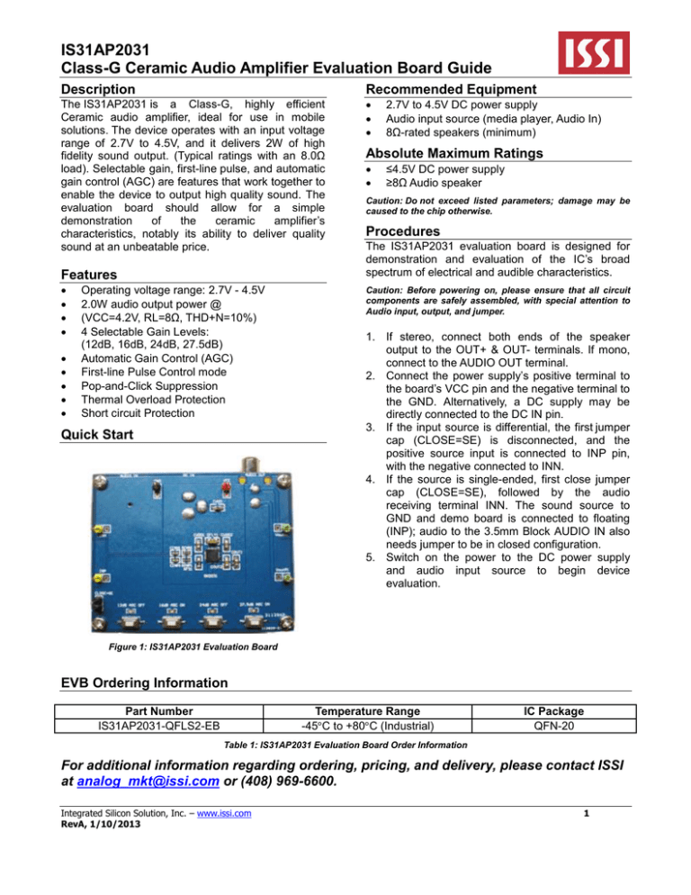
1. If stereo, connect both ends of the speaker
output to the OUT+ & OUT- terminals. If mono,
connect to the AUDIO OUT terminal.
2. Connect the power supply’s positive terminal to
the board’s VCC pin and the negative terminal to
the GND. Alternatively, a DC supply may be
directly connected to the DC IN pin.
3. If the input source is differential, the first jumper
cap (CLOSE=SE) is disconnected, and the
positive source input is connected to INP pin,
with the negative connected to INN.
4. If the source is single-ended, first close jumper
cap (CLOSE=SE), followed by the audio
receiving terminal INN. The sound source to
GND and demo board is connected to floating
(INP); audio to the 3.5mm Block AUDIO IN also
needs jumper to be in closed configuration.
5. Switch on the power to the DC power supply
and audio input source to begin device
evaluation.
Figure 1: IS31AP2031 Evaluation Board
EVB Ordering Information
Part Number
IS31AP2031-QFLS2-EB
Temperature Range
-45°C to +80°C (Industrial)
IC Package
QFN-20
Table 1: IS31AP2031 Evaluation Board Order Information
For additional information regarding ordering, pricing, and delivery, please contact ISSI
at analog_mkt@issi.com or (408) 969-6600.
Integrated Silicon Solution, Inc. – www.issi.com
RevA, 1/10/2013
1
IS31AP2031
Class-G Ceramic Audio Amplifier Evaluation Board Guide
Device Operation
The device enables high level of sound fidelity
output in part because of its low operating frequency.
Lines are copper wire with 0.75mm diameter. Audio
signal interference filters compensate for any
distortions in input signal. The signal filters are
situated close to the speaker and away from RFsensitive components, specifically the boost
converter, to minimize EMI. A cooling plate beneath
the chip on the PCB facilitates efficient thermal
dissipation. The capacitors are located near the
OUT+ and OUT- pins. The recommended wire
diameter specification is greater than or equal to
0.55mm.
additional operational information can be referenced
in the IS31AP2031 datasheet.
Mode A: Gain = 12.0 dB, AGC = ON
Mode B: Gain = 16.0 dB, AGC = ON
Mode C: Gain = 24.0 dB, AGC = ON
Mode D: Gain = 27.5 dB, AGC = ON
High-pass filter
The input resistance (RINN1) and input capacitance
(CINN1), as seen in Figure 2’s Schematic, constitute
a high-pass filter with a specific cut-off frequency,
denoted by
. For modes A and B, the cut-off
frequency is determined by solving equation (1).
(1)
Gain Selection
IS31AP2031 has four modes of operation; the
configuration is done via the first-line pulse control
SDB pin on the evaluation board. A 4-button switch
allows for easy mode changing, and a signal lamp
will indicate which mode is currently on. The default
mode is 4: (gain of 27.5dB, and open the AGC), and
For modes C and D, the cut-off frequency can be
found by using the following equation (2).
(2)
The input capacitance plays a critical role in the level
of bass present at the device outputs.
VDD1
C1
1uF
C2
0.1uF
5
C3
0.1uF
U34
Vout
BP
4
Vdd GNDEN
1
2
U1
VCC
3
SDB
VCC
CVDD
10uF
VDD1
VDD1
U2
R1
1K
1
R2
1K
2
3
4
5
6
7
27.5dB AGC ON
24dB AGC OFF
8
16dB AGC ON
9
12dB AGC OFF
10
R10
10K
P0.0
P0.1
P1.7
P0.2
P1.6
P0.3
RST
P0.4
GND
P0.5
OSC1
OSC2
VDD
P0.6
20
R4
1K
19
R3
1K
18
VDD
AVIN
CVDD2
0.1uF
CVDD1
10uF
RINN1
CINN1
15nF 10K
RINP1
CINP1
15nF 10K
CLOSE=SE
15,21,24
COUT2
0.1uF
1
9
10
SDB
CP
CN
Jumper
3
26
CFLY1
4.7uF
INOUT+
20
IN+
OUT-
13
COUT1
10uF
FS
GND
100K RFS1
16
Speaker
18,27
GND
IS31AP2031
SDB
17
16
15
R6
100K
VDD1
14
INT1/P1.4
13
T1/P0.7
INT0/P1.3
12
TXD/P1.0
11
T0/P1.2 RXD/P1.1
R9 R8 R7
10K10K10K
VDD1
Figure 2: IS31AP2031 Evaluation Board Circuit Schematic
Integrated Silicon Solution, Inc. – www.issi.com
RevA, 1/10/2013
2
IS31AP2031
Class-G Ceramic Audio Amplifier Evaluation Board Guide
Bill of Materials
Name
Symbol
Description
Qty
Supplier
Capacitor
CVDD,CVDD1,COUT1
Capacitor
Part No.
10.0μF±10% 10V
3
-
-
CVDD2,COUT2
0.1μF±10% 10V
2
-
-
Capacitor
CINN1,CINP1
15nF±10%,10V
2
-
-
Resistor
RINN1,RINP1
10kΩ±5%
2
-
-
Resistor
RFS1
100kΩ±5%
1
-
-
Capacitor
CFLY1
4.7μF±10%
1
-
-
Audio Amplifier
U1
Class-G Ceramic
1
ISSI
IS31AP2031-QFLS2-TR
Table 2: Bill of Materials. Please refer to schematic and device datasheet for more information.
Figure 3: PCB Component Placement Guide- Topside
Integrated Silicon Solution, Inc. – www.issi.com
RevA, 1/10/2013
3
IS31AP2031
Class-G Ceramic Audio Amplifier Evaluation Board Guide
Figure 4: PCB Layout- Topside
Figure 5: PCB Layout- Underside
Integrated Silicon Solution, Inc. – www.issi.com
RevA, 1/10/2013
4
IS31AP2031
Class-G Ceramic Audio Amplifier Evaluation Board Guide
Figure 6: PCB Component Placement Guide- Underside
Copyright © 2013 Integrated Silicon Solution, Inc. All rights reserved. ISSI reserves the right to make changes to this specification
and its products at any time without notice. ISSI assumes no liability arising out of the application or use of any information,
products or services described herein. Customers are advised to obtain the latest version of this device specification before relying
on any published information and before placing orders for products.
Integrated Silicon Solution, Inc. does not recommend the use of any of its products in life support applications where the failure or
malfunction of the product can reasonably be expected to cause failure of the life support system or significantly affect its safety or
effectiveness. Products are not authorized for use in such applications unless Integrated Silicon Solution, Inc. receives written
assurance to its satisfaction, that:
a.) the risk of injury or damage has been minimized;
b.) the user assume all such risks; and
c.) potential liability of Integrated Silicon Solution, Inc is adequately protected under the circumstances.
Integrated Silicon Solution, Inc. – www.issi.com
RevA, 1/10/2013
5


