Understanding the Effect of Clock Jitter on High Speed ADCs
advertisement

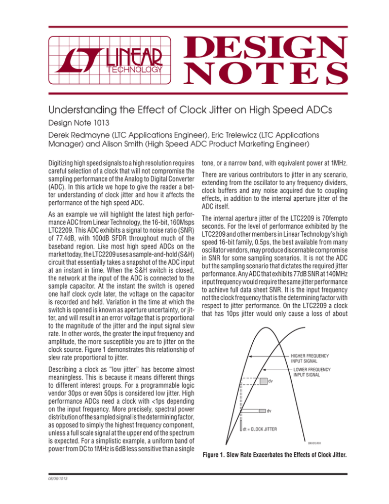
advertisement Understanding the Effect of Clock Jitter on High Speed ADCs Design Note 1013 Derek Redmayne (LTC Applications Engineer), Eric Trelewicz (LTC Applications Manager) and Alison Smith (High Speed ADC Product Marketing Engineer) Digitizing high speed signals to a high resolution requires careful selection of a clock that will not compromise the sampling performance of the Analog to Digital Converter (ADC). In this article we hope to give the reader a better understanding of clock jitter and how it affects the performance of the high speed ADC. As an example we will highlight the latest high performance ADC from Linear Technology, the 16-bit, 160Msps LTC2209. This ADC exhibits a signal to noise ratio (SNR) of 77.4dB, with 100dB SFDR throughout much of the baseband region. Like most high speed ADCs on the market today, the LTC2209 uses a sample-and-hold (S&H) circuit that essentially takes a snapshot of the ADC input at an instant in time. When the S&H switch is closed, the network at the input of the ADC is connected to the sample capacitor. At the instant the switch is opened one half clock cycle later, the voltage on the capacitor is recorded and held. Variation in the time at which the switch is opened is known as aperture uncertainty, or jitter, and will result in an error voltage that is proportional to the magnitude of the jitter and the input signal slew rate. In other words, the greater the input frequency and amplitude, the more susceptible you are to jitter on the clock source. Figure 1 demonstrates this relationship of slew rate proportional to jitter. Describing a clock as “low jitter” has become almost meaningless. This is because it means different things to different interest groups. For a programmable logic vendor 30ps or even 50ps is considered low jitter. High performance ADCs need a clock with <1ps depending on the input frequency. More precisely, spectral power distribution of the sampled signal is the determining factor, as opposed to simply the highest frequency component, unless a full scale signal at the upper end of the spectrum is expected. For a simplistic example, a uniform band of power from DC to 1MHz is 6dB less sensitive than a single tone, or a narrow band, with equivalent power at 1MHz. There are various contributors to jitter in any scenario, extending from the oscillator to any frequency dividers, clock buffers and any noise acquired due to coupling effects, in addition to the internal aperture jitter of the ADC itself. The internal aperture jitter of the LTC2209 is 70fempto seconds. For the level of performance exhibited by the LTC2209 and other members in Linear Technology’s high speed 16-bit family, 0.5ps, the best available from many oscillator vendors, may produce discernable compromise in SNR for some sampling scenarios. It is not the ADC but the sampling scenario that dictates the required jitter performance. Any ADC that exhibits 77dB SNR at 140MHz input frequency would require the same jitter performance to achieve full data sheet SNR. It is the input frequency not the clock frequency that is the determining factor with respect to jitter performance. On the LTC2209 a clock that has 10ps jitter would only cause a loss of about HIGHER FREQUENCY INPUT SIGNAL LOWER FREQUENCY INPUT SIGNAL dv dv dt = CLOCK JITTER DN1013 F01 Figure 1. Slew Rate Exacerbates the Effects of Clock Jitter. 08/06/1013 0.7dB SNR at an input frequency of 1MHz. At 140MHz the SNR would degrade to 41.1dB. Figure 2 demonstrates the effects of clock jitter on the SNR of the LTC2209 as a function of sampled input frequency with a family of curves of increasing clock jitter from a perfect clock to 100ps of jitter. At 100ps, the ADC SNR begins to degrade with input frequencies of only 200kHz! OSC JITTER 0fs SNR (dB) 70 500fs Power Density (one phase modulation sideband) (4) 1ps 50 Carrier Power 2ps 40 (3) L ( f) = 200fs 60 V(t) = [VO + ε(t)]sin[2πfOt + ϕ(t)] The spectral density denoted as L(f) is stated as the ratio of the single sideband phase noise power in a 1Hz bandwidth at an offset frequency, also called the Fourier frequency, relative to the carrier power, equation (4). 90 80 phase noise, equation (3). The spectral density measurements assume the AM component ε(t) of the noise is negligible compared to the phase noise component ϕ(t). This is a reasonable assumption with any quality frequency source. 5ps Jitter is the integral of spectral phase density with respect to frequency between two limits in frequency and expressed in time, equation (5). The result is frequency independent. 10ps 30 100ps 20 1 10 100 INPUT FREQUENCY (MHz) 20ps 50ps 1000 DN1013 F02 σ= Figure 2 Jitter Degradation of SNR as a Function of Input Frequency The theoretical limit on SNR resulting from clock jitter is given as equation (1) SNR(dBFS) = –20log(2πfinσ) (1) where fin is the input frequency and σ is the jitter in RMS seconds. The jitter related noise power is proportional to the input power (dBFS). As the input level is raised or decreased the noise component related to jitter changes accordingly. If, for example, we have a –1dBFS input signal at a 70MHz IF, sampled by a clock with 1ps jitter we can expect an SNR of 68dBFS. At –5dBFS, the noise component related to jitter would drop 4dB to an SNR of 72dBFS. To calculate the total SNR degradation we add the jitter noise power to the published SNR of the ADC, equation (2): SNR degradation (dBFS) = 10log ( 10(–SNRadc/10) + 10(–SNRjitter/10)) (2) Understanding Clock Oscillator Jitter Specs. Clock oscillators are usually specified in terms of spectral density of phase noise in dBc/Hz. An oscillator output can be decomposed into an amplitude term with associated amplitude noise and a frequency term with associated 1 2πfO f ∫f2 2L ( f ) df (5) 1 Most oscillators that rate jitter are rated between 12kHz and 20MHz. This is due to historical reasons related to optical communications and is not applicable to most other practical cases. Performance may in fact fall apart beyond these limits so take care not to be lured in without careful examination. For many oscillators where close-in phase noise dominates, the lower limit has the most impact on the published figure. While this expression is convenient as it yields a single number useful for calculation of ADC SNR degradation, it is not as informative as the spectral density. For example, two oscillators having different spectral content may have the same jitter over the same integration limits but may not produce the same SNR. Elevated wideband noise may not produce a poor jitter spec, but will degrade SNR. Close-in phase noise causes the fundamental signal to spread into adjacent frequency bins of an FFT reducing dynamic range, whereas broadband phase noise will uniformly elevate the noise floor throughout the entire Nyquist zone thus reducing the overall SNR performance of the ADC. Jitter does not affect SFDR unless the clock also contains spurs. The lower frequency limit of integration should correspond to the frequency resolution of any manipulations of the sampled data- as the size of an FFT increases for example. Figure 3 shows the effect of band limited clock jitter related to phase modulation of two signals of similar amplitude, but of different frequency. This illustrates the exaggerated effect of both random phase noise and phase modulation of the clock in the presence of higher input frequencies. The clock input of the ADC should be regarded as the local oscillator port of the ADC, not a digital control signal. Anything present on the clock, including wideband noise extending to GHz frequencies, will mix with the input signal. 0 THE HIGHER THE INPUT FREQUENCY, THE MORE SENSITIVE TO PHASE MODULATION OF THE CLOCK –20 dB –40 –60 –80 –100 –120 1 73 145 217 289 BINS 361 433 505 DN1013 F03 Figure 3. Effect of Clock Phase Noise on Input Frequency The Application Determines the Needs, Not the ADC Applications that are receiving weak signals in close proximity to strong tones, e.g. static reflections in Doppler ultrasound, radar and RFID are sensitive to close-in phase noise. A digital radio where strong interferers (single tones) may appear in close proximity, or may be much stronger than a signal of interest, is generally demanding in terms of close-in phase noise, and may be sensitive to wideband phase noise. As any wideband signal source tends to have a high crest factor, and requires headroom for interferers, the nominal power at the ADC may be low. The characteristics of the band of interest must be taken into consideration in deciding on a clock source. Selecting an Oscillator to Drive High Speed ADCs: Most oscillators will have close-in phase noise that will limit the dynamic range close to a strong fundamental. If close-in phase noise is important, based on your dynamic range requirement in proximity to strong tones, you may need a PLL (Phase Locked Loop) to reduce the close-in noise of your oscillator source or to lock your oscillator to an accurate frequency reference. The use of a PLL as a jitter cleaner essentially provides a very narrowband tracking filter. Your choice of oscillator will dictate your loop bandwidth, as well; your desired loop BW will dictate the oscillator. A VCXO (voltage controlled crystal oscillator) requires only a narrow loop bandwidth to track a stable reference. VCOs can provide wide tuning range, but need wider loop BW in order to reduce their close-in phase noise to acceptable levels. If you only require a very restricted tuning range, perhaps locking to a reference oscillator, the use of a VCXO is the best option. If you need the octave tuning range of a VCO, and need low close-in phase noise, you may have a problem, especially if you need high divider ratios and low reference comparison frequencies in your PLL. Figure 4 shows a comparison of a typical VCXO vs VCO High symbol rate communications applications are generally not sensitive to close-in phase noise, and may not be overly sensitive to the effects of wideband phase noise. High crest factor waveforms (WCDMA OFDM) with relatively even power distribution have a low RMS power level, and also require headroom, so will not elevate the noise floor as much as a full amplitude single tone. However higher order modulation types, QAM and M-nary phase modulation are more susceptible to noise and have more narrow carrier recovery loop bandwidths for the same symbol rates as for example QPSK used in CDMA systems. L (dBc/Hz) Conversely, when digitizing a CCD output, jitter generally doesn’t matter due to the low slew rate at the point in time sampling occurs. Video applications are also not very sensitive. For example, in HDTV the sample window is approximately 6400ps (time per pixel). –30 –40 –50 –60 –70 –80 –90 –100 –110 –120 –130 –140 –150 –160 –170 –180 –190 –200 IMPLIED LOOP BW FOR 10MHz REFERENCE MULTIPLIED TO 100MHz VCO VCXO 10 100 10k 1k FREQUENCY (Hz) 100k 1M DN1013 F04 Figure 4. Comparison of Typical VCXO Versus Typical VCO Phase Noise Performance phase noise plot. The optimal loop bandwidth for the PLL is suggested by the intersection of the noise density of the reference oscillator as multiplied by the center frequency, and the phase noise plot of the VCXO or VCO. The example would suggest 2kHz for the VCXO, and 300kHz for the VCO. A 300kHz corner requires a comparison frequency of at least 3MHz which suggests 5MHz. The VCXO could be used with a comparison frequency as low as 20kHz. If a lower frequency reference were used (high divide ratios) with the VCO, the intersection of the multiplied phase noise with that of the VCO would be at a lower frequency, substantially increasing the jitter. The use of an excessively low loop BW with a lower multiplication ratio will cause the phase noise of a VCO to remain within the loop BW. If your application is insensitive to close-in phase noise, and does not need to be locked to a reference, an XO can be used. Clock Sources and Clock Architectures A good clock can be compromised by routing it through an FPGA where internal crosstalk is prevalent. FPGAs often maximize I/Os at the expense of ground pins, resulting in ground bounce. If the FPGA is driving outputs at different GOOD rates, these will manifest themselves in any clock routed through the FPGA and ultimately on the output of any ADC using that clock. A low noise flip-flop clocked by the clean VCO signal can be used as a retiming stage to eliminate jitter when an FPGA is used to frequency divide the VCO. The FPGA can be used to implement a narrow band PLL for an external VCXO, with an external loop filter, and a loop filter driver protected from reflected ground bounce from the FPGA. Do not use a DLL to produce a clock for an ADC unless you are over-sampling the audio band. A good clock can also be compromised by routing it among digital signals. Any clock originating any distance from the ADC must be routed through a conduit of copper and vias. Figure 5 shows examples of good and bad routing of clocks. The bad cases are where the clocks are within cavities shared with digital signals. Conclusion The impact of jitter on ADC performance is a function of input frequency (slew rate) not sample rate. The choice of clock source will be determined by the application. Don’t always believe the clock source vendors. Test your clock sources with your ADC evaluation board before it is too late. BAD DN1013 F05 CLOCK OFFENDERS Figure 5. Example of Good and Bad Layout for Clock Routing. Data Sheet Download For applications help, call (408) 432-1900, Ext. 2360 www.linear.com Linear Technology Corporation dn1013f LT 0906 • PRINTED IN THE USA FAX: (408) 434-0507 ● www.linear.com © LINEAR TECHNOLOGY CORPORATION 2006 1630 McCarthy Blvd., Milpitas, CA 95035-7417 (408) 432-1900 ●


