Iraqi Journal of Applied Physics
Haitham S. Dawood
School of Applied Sciences,
University of Technology,
Baghdad, Iraq
Analytical Equivalent
Circuit of High-Irradiated
Conventional Silicon
Solar Cell Performance
In this study the current–voltage characteristics of a conventional silicon solar
cell were studied. The experimental examination is carried out under a high
concentration of light. The variations of the two reverse saturation currents
are consistent with the physical significance of both the diffusion and the
space-charge generation-recombination terms through their exponential
variations. The simulation results clearly demonstrated that the solar cell is
described with reasonable accuracy by a two-diode equivalent model that
simulates the effects of the double-exponential dark current–voltage
characteristics on the open-circuit voltage, fill factor, and conversion
efficiency of the solar cell at a high concentration. The theoretical results are
in good agreement with the experimental observations.
Keywords: Solar cells, Silicon-based devices, Equivalent circuit, High irradiation
Received: 20 July 2009, Revised: 22 September 2009, Accepted: 27 September 2009
1. Introduction
The presence of a p-n junction in a
semiconductor makes solar power possible. The
space charge region is formed as a result of the
diffusion of majority carriers across the
metallurgical junction, and its width is fixed
when the diffusion is counter balanced by the
drift of carriers in the opposite direction, thus
setting up a compact but strong electric field as
the collecting junction in the depletion region
[1]. In thermal equilibrium, drift and diffusion
currents through the depletion region oppose
each other, resulting in zero net current flow.
Using light as an external stimulus allows the p-n
junction to behave as follows. Part of the solar
spectrum is absorbed in a semiconductor through
the transfer of optical energy to electrons that are
excited into the conduction band creating holes
in the valence band. The electric field in the
depletion region helps in separating these
electron-hole pairs, resulting in a voltage or the
photovoltaic effect [2].
The efficiency of photovoltaic solar cells
decreases with an increase in temperature [3].
When silicon solar cells are used under
concentrated sunlight they tend to heat up [4], as
a result of which the current and voltage
generated by the solar cell are modified. An
excessive rise in the solar cell temperature has
degrades effects on the solar cell characteristics.
In general, the open-circuit voltage (VOC)
decreases rapidly and the short circuit current
(ISC) increases slowly, as the temperature rises.
In this paper, we present a modeling analysis
implemented to introduce the I–V characteristics
of silicon-based solar cells at high light
All rights reserved
concentration.
The correlations between
experimental I–V plots and theoretical
counterparts under different illumination
intensities are studied.
The model must take into account the various
recombination and generation processes in the
solar cell under illumination. Thus, the device
can be modeled with either the conventional
single-diode model or the two-diode model.
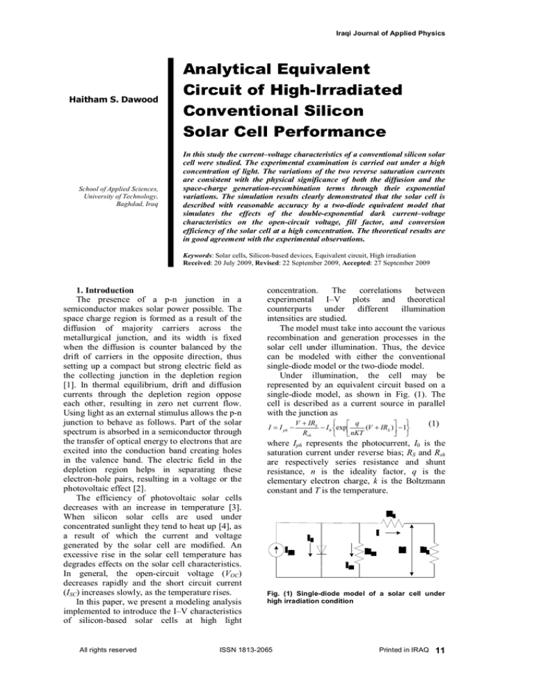
Under illumination, the cell may be
represented by an equivalent circuit based on a
single-diode model, as shown in Fig. (1). The
cell is described as a current source in parallel
with the junction as
V + IRS
q
(1)
I=I
I exp
(V + IR ) 1
ph
Rsh
0
nKT
S
where Iph represents the photocurrent, I0 is the
saturation current under reverse bias; RS and Rsh
are respectively series resistance and shunt
resistance, n is the ideality factor, q is the
elementary electron charge, k is the Boltzmann
constant and T is the temperature.
Fig. (1) Single-diode model of a solar cell under
high irradiation condition
ISSN 1813-2065
Printed in IRAQ
11
IJAP Vol. (5), No. (4), October 2009
The simplified two-diode model of a solar
cell may be described by the new lumped
parameter simplified equivalent circuit shown in
Fig. (2) [5,6]. For a given incident light intensity,
at a given temperature, the implicit I–V
relationship is given by
V + IR S
R sh
I = I ph
I 01 {exp[B1 (V + IR S )] 1}
I 02 {exp[B 2 (V + IR S )] 1}
(2)
where B1=q/kT, B2=B1/n and I01 represents the
saturation current originating from the quasi
neutral region of the junction which is affected
by, as diffusion, recombination and the drift
effect [5]; I02 corresponds to the carrier
recombination via deep levels in the spacecharge region of the junction [6]. The reverse
saturation current I02 is generally 3 to 7 orders of
magnitude larger than I01; the diode quality factor
n=2 for the approximation corresponding to the
Shockley–Read–Hall recombination current in
the space-charge region [5,7]; n is also a fitting
parameter that is greater than 2.
illumination. It should be noted that the
illumination does not cause a simple translation
of the I–V characteristics along the current axis
[9,10], the series resistance effect is non-linear
and the injection level changes from low to high
level. Several methods have been proposed for
the determination of the free parameters in this
model from the I–V measurements [11,12].
In order to present general approach for
calculating all the cell parameters, we use Eq.
(2), for the two following special cases.
(i) For V=VOC and I=0
VOC
0 = I ph
I 01 {exp[B1 (VOC + IRS )] 1}
Rsh
(3)
I 02 {exp[B2 (VOC + IRS )] 1}
(ii) For I=ISC and V=0
I sh RS
I SC = I ph
I 01 {exp[B1 ( I SC RS )] 1}
Rsh
(4)
I 02 {exp[B2 ( I SC RS )] 1}
Differentiating Eq. (2) with respect to I on
both sides for the two special cases considered
above we have
(i) For I=0, V=VOC, one can write
1=
dV
dI
+ RS
V =VOC
I 02 B2 exp[B2 (VOC )])
where
Fig. (2) Double-diode model of a solar cell under
high irradiation condition
RS 0 =
dV
dI
1
Rsh
I 01 B1 exp[B1 (VOC ) ]
(5a)
V =VOC
Thus, RS is given as
1
dV
The experimental study of the temperature
+ RS
+ I 01 B1 exp[B1 (VOC )]
1=
dependence of I01 and I02 should help to verify
dI V =VOC
Rsh
their different origins. Such studies have been
(5b)
+ I 02 B2 exp[B2 (VOC )])
previously published under dark conditions [8].
It is interesting to determine the temperature
dependencies of electrical parameters while the
cell is operating as a generator under
_____________________________________________________________________________________
Re-arranging
dV
dI
RS =
V =VOC
1
1
1
+ I 01B1 exp[B1 (VOC )] + I 02 B2 exp[B2 (VOC )]
Rsh
(ii) For V=0, I=ISC, we obtain
RS = RS 0
1=
dV
dI
+ RS
I = I SC
1
Rsh
I 01 B1 exp[B1 ( I SC RS )] I 02 B2 exp[B2 ( I SC RS )]
where
Rsh 0 =
12
dV
dI
(5c)
1
+ I 01 B1 exp[B1 (VOC )] + I 02 B2 exp[B2 (VOC )]
Rsh
I = I SC
© 2009 Iraqi Society for Alternative and Renewable Energy Sources and Techniques (I.S.A.R.E.S.T.)
(6)
(7)
Iraqi Journal of Applied Physics
Thus
1
RS =
1
Rsh 0
RS
(8)
I 01 B1 exp[B1 ( I SC RS )] I 02 B2 exp[B2 ( I SC RS )]
For V=VOC and I=ISC, we have
I ph =
VOC
+ I 01{exp[B1VOC ] 1} I 02 {exp[B2VOC ] 1}
Rsh
(9)
Equations (3), (4), (6), (8), and (9) form a system of simultaneous equations where the unknown
parameters are RS, Rsh, I01, I02, and Iph respectively. To be very general, let
u=RS, v=Rsh, x=Iph, y=I01, z=I02
(10)
The system can be written as
f1 (u , v, x, y, z ) = 0
f 2 (u , v, x, y, z ) = 0
f 3 (u , v, x, y, z ) = 0
f 4 (u, v, x, y, z ) = 0
f5 (u, v, x, y, z ) = 0
(11)
The system in Eq. (11) is resolved numerically using the Newton–Raphson algorithm of the form
vk
vk 1
wk 1
wk
xk = xk 1
yk 1
yk
zk
zk 1
f1
u
f2
u
f3
u
f4
u
f5
u
f1
v
f2
v
f3
v
f4
v
f5
v
f1
x
f2
x
f3
x
f4
x
f5
x
f1
y
f2
y
f3
y
f4
y
f5
y
f1
z
f2
z
f3
z
f4
z
f5
z
1
.
f1 (u k 1 , vk 1 , xk 1 , yk 1 , z k 1 )
f 2 (u k 1 , vk 1 , xk 1 , yk 1 , z k 1 )
f 3 (u k 1 , vk 1 , xk 1 , y k 1 , z k 1 ) . (12)
f 4 (u k 1 , vk 1 , xk 1 , yk 1 , z k 1 )
f 5 (u k 1 , vk 1 , xk 1 , yk 1 , z k 1 )
( u k 1 ,vk 1 , xk 1 , yk 1 , z k 1 )
_____________________________________________________________________________________
where the initial conditions are thus given by
u (1)
v(1)
0
0
x(1) = 0
0
y (1)
z (1)
0
(13)
The five different parameters of the singlediode model, can be determined directly from the
latter equations using I01=0 and I02=I0.
2. Experiment
In this work, we have used standard solar
panel fabricated by Hebe Solar Co., Ltd. (China)
in order to test the model at optimum solar
parameters. The panel is 15x15cm in area and
partitioned into many multicrystalline silicon p-n
junction solar cells. Each cell is 25x25mm in
dimensions, 300Um in thickness and delivers
40% more power than customary cells. The front
grid was made of 2 silver bus bars, 1mm wide,
with about 80 fingers of 5Um length between
All rights reserved
them and SiNx AR coating. The back side
contains of 5mm wide soldering pads (Ag/Al)
and back surface field (Al). The contact
thickness was 2.5Um and the sheet resistance
was 900 /V. The cells were mounted on
thermal-clad substrates, which are commonly
used for hybrid electronic circuits. The n-type
side was 200nm thick with a doping density of
2x1018cm-3 and the p-type side was 800nm thick
with a doping density of 2x1017cm-3. The
maximum efficiency of this cell as illustrated by
the manufacturer is ranging within 13.8-15.6% at
3.5W maximum output power. The conversion
measurements were conducted under solar
radiation. The concentrator system used is
advantageous for giving good illumination
uniformity at the focus. The focus was 3X3cm2
in area and was slightly larger than the
dimensions of the tested cells.
The measured parasitic resistance induced by
this set-up was in the order of 20m which is a
minimal contribution for the tested cells. Under
the same experimental conditions, a solar cell
ISSN 1813-2065
Printed in IRAQ
13
IJAP Vol. (5), No. (4), October 2009
operating at a high concentration of light shows
only slight degradation as a result of the parasitic
effect.
8
7
Current (mA)
Current (A)
0.6
0.4
2 diode
1 diode
exp.
0.2
0
0
0.4
0.8
1.2
1.6
Voltage (V)
Fig. (5) Simulated curves and experimental
measurements of I–V characteristics of the solar
cell under concentration level of X=139:27 (X is the
light concentration level)
1.8
1.6
1.4
1.2
1
0.8
2 diode
1 diode
exp.
0.4
5
0.2
4
0
0
3
0.4
0.8
1.2
1.6
Voltage (V)
2
2 diode
1 diode
exp.
1
0
0
0.4
0.8
1.2
1.6
Voltage (V)
Fig. (3) Simulated curves and experimental
measurements of I–V characteristics of the solar
cell under concentration level of X=1 (X is the light
concentration level)
500
450
400
350
Current (mA)
0.8
0.6
6
300
250
200
150
2 diode
1 diode
exp.
100
50
0
0
0.4
0.8
1.2
1.6
Voltage (V)
Fig. (4) Simulated curves and experimental
measurements of I–V characteristics of the solar
cell under concentration level of X=73:36 (X is the
light concentration level)
14
1
Current (A)
3. Results and Discussion
The equivalent-circuit parameter values were
determined and the simulated I–V plots together
with the experimental counterparts are
represented in Figs. (3–6) for four different
concentrations. The simulated parameters were
calculated using the single-diode model and the
two-diode model
presented above.
A
Comparison between the cell parameters
obtained using each model with the
corresponding
experimental
values
was
conducted to find the best model.
The results clearly show that the proposed
two-diode model is compatible with the solar cell
at high concentrations (X=73:36, 139.27, and
201.19). On the other hand, the single-diode
model seems better for the low concentration of
X=1 where the two-diode model is less precise
than the single-diode model.
1.2
Fig. (6) Simulated curves and experimental
measurements of I–V characteristics of the solar
cell under concentration level of X=201:19 (X is the
light concentration level)
At high levels of solar concentration, the
good agreement of experimental results with the
two-diode model can be explained by the fact
that under such conditions the traps, which are
susceptible to intervening in the recombination,
are saturated and the amount of diffusion
becomes significant. The two-diode model can
be applied under conditions of weak injection,
while taking in account three essential
mechanisms [7]. First, the diffusion takes into
account the recombination mechanisms in the
quasi-neutral regions (notably the contacts).
Second, the recombination in the space-charge
region of the junction, by the recombinant
centers associated with the levels situated in the
strip forbidden for a homojunction represented
by one exponential term. Finally, Joule effect is
translated into losses due to the series resistance
and shunt resistance.
Therefore the two-diode model is the more
suitable for the precise simulation of a solar cell
in a real situation [1,5,10]. This is presumably
due to the minority carrier diffusion process,
© 2009 Iraqi Society for Alternative and Renewable Energy Sources and Techniques (I.S.A.R.E.S.T.)
Iraqi Journal of Applied Physics
[2] T.K.P. Wong, Electron. Lett., 32(3) (1996)
252 – 253.
[3] D. Meneses-RodrXguez, P.P. Horley, J.
Gonzalez-Hernandez, Y.V. Vorobiev and
P.N. Gorley, Solar Energy, 78 (2005) 243.
4. Conclusions
[4] R.V. Singh and C.M. Singal, Solar Cells, 10
The effects of double-exponential dark
(1983) 155.
current–voltage characteristics on the different
[5] T.K.P. Wong and P.C.H. Chan, An
parameters of a silicon-based solar cell operating
equivalent circuit approach to solar cell
at high concentration of light were studied. The
modeling, IEEE Region 10 Inter. Conf. on
two-diode model was compared to the singleMicroelectronics and VLSI, 1995, TENCON
diode one in terms of the agreement between the
95, 6-10 (November 1995) 222-225.
simulated cell parameters and experimental
[6] G.L. Araujo, E. Sanchez and M. Marti,
values. We conclude that the conventional
Solar Cells, 5 (1982) 199.
single-diode model is inadequate for describing
[7] J.-P. Charles, A. Haddi, A. Maouad, H.
the behavior of the studied device under high
Bakhtiar, A. Zerga, A. Hoffmann and P.
light concentration and that the two-diode model
Mialhe, Rev. Energy Ren., 3 (2000) 1.
is more appropriate.
[8] F. Lindholm, J. Fossum and E. Burgess,
IEEE Trans. Electron. Devices, 26 (1979)
Acknowledgment
165.
Author would like to thank Dr. R.M. Ibrahim
[9] R.N. Hall, Solid State Electron., 24 (1981)
for his valuable comments and notes. He also
595.
would like to thank Prof. M.A. Habeeb for his
[10] J.-P. Charles, I. Mekkaoui-Alaoui and G.
assistance in numerical analysis. Finally, he
Bordure, Solid State Electron., 28 (1985)
thanks Mr. S.I. Al-Hadithi at Thin Films
807.
Laboratory, University of Baghdad for
[11] R.A. Kumar, M.S. Suresh and J. Nagaraju,
experimental assistance and measurements.
IEEE Trans. on Electron. Devices, 48(9)
(2001) 2177-2179.
References
[12] A. Cheknane, H.S. Hilal, F. Djeffal, B.
[1] M. Masaki and M. Tatsuo, Jpn. J. Appl.
Benyoucef and J.-P. Charles, Microelectron.
Phys. Part 1, 45(1B) (2006) 542-545.
J., 39(10) (2008) 1173-1180.
_____________________________________________________________________________________
which becomes dominant in the conduction
mechanisms at a high concentration of light
[1,2].
All rights reserved
ISSN 1813-2065
Printed in IRAQ
15

