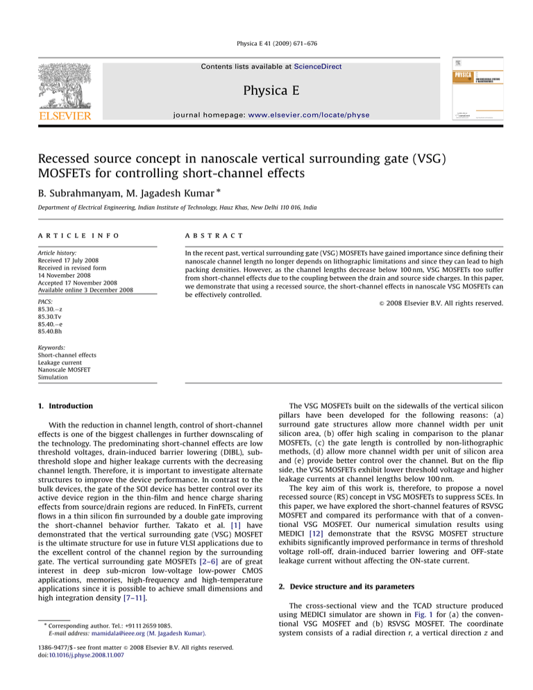
ARTICLE IN PRESS
Physica E 41 (2009) 671–676
Contents lists available at ScienceDirect
Physica E
journal homepage: www.elsevier.com/locate/physe
Recessed source concept in nanoscale vertical surrounding gate (VSG)
MOSFETs for controlling short-channel effects
B. Subrahmanyam, M. Jagadesh Kumar Department of Electrical Engineering, Indian Institute of Technology, Hauz Khas, New Delhi 110 016, India
a r t i c l e in fo
abstract
Article history:
Received 17 July 2008
Received in revised form
14 November 2008
Accepted 17 November 2008
Available online 3 December 2008
In the recent past, vertical surrounding gate (VSG) MOSFETs have gained importance since defining their
nanoscale channel length no longer depends on lithographic limitations and since they can lead to high
packing densities. However, as the channel lengths decrease below 100 nm, VSG MOSFETs too suffer
from short-channel effects due to the coupling between the drain and source side charges. In this paper,
we demonstrate that using a recessed source, the short-channel effects in nanoscale VSG MOSFETs can
be effectively controlled.
& 2008 Elsevier B.V. All rights reserved.
PACS:
85.30.z
85.30.Tv
85.40.e
85.40.Bh
Keywords:
Short-channel effects
Leakage current
Nanoscale MOSFET
Simulation
1. Introduction
With the reduction in channel length, control of short-channel
effects is one of the biggest challenges in further downscaling of
the technology. The predominating short-channel effects are low
threshold voltages, drain-induced barrier lowering (DIBL), subthreshold slope and higher leakage currents with the decreasing
channel length. Therefore, it is important to investigate alternate
structures to improve the device performance. In contrast to the
bulk devices, the gate of the SOI device has better control over its
active device region in the thin-film and hence charge sharing
effects from source/drain regions are reduced. In FinFETs, current
flows in a thin silicon fin surrounded by a double gate improving
the short-channel behavior further. Takato et al. [1] have
demonstrated that the vertical surrounding gate (VSG) MOSFET
is the ultimate structure for use in future VLSI applications due to
the excellent control of the channel region by the surrounding
gate. The vertical surrounding gate MOSFETs [2–6] are of great
interest in deep sub-micron low-voltage low-power CMOS
applications, memories, high-frequency and high-temperature
applications since it is possible to achieve small dimensions and
high integration density [7–11].
Corresponding author. Tel.: +9111 2659 1085.
E-mail address: mamidala@ieee.org (M. Jagadesh Kumar).
1386-9477/$ - see front matter & 2008 Elsevier B.V. All rights reserved.
doi:10.1016/j.physe.2008.11.007
The VSG MOSFETs built on the sidewalls of the vertical silicon
pillars have been developed for the following reasons: (a)
surround gate structures allow more channel width per unit
silicon area, (b) offer high scaling in comparison to the planar
MOSFETs, (c) the gate length is controlled by non-lithographic
methods, (d) allow more channel width per unit of silicon area
and (e) provide better control over the channel. But on the flip
side, the VSG MOSFETs exhibit lower threshold voltage and higher
leakage currents at channel lengths below 100 nm.
The key aim of this work is, therefore, to propose a novel
recessed source (RS) concept in VSG MOSFETs to suppress SCEs. In
this paper, we have explored the short-channel features of RSVSG
MOSFET and compared its performance with that of a conventional VSG MOSFET. Our numerical simulation results using
MEDICI [12] demonstrate that the RSVSG MOSFET structure
exhibits significantly improved performance in terms of threshold
voltage roll-off, drain-induced barrier lowering and OFF-state
leakage current without affecting the ON-state current.
2. Device structure and its parameters
The cross-sectional view and the TCAD structure produced
using MEDICI simulator are shown in Fig. 1 for (a) the conventional VSG MOSFET and (b) RSVSG MOSFET. The coordinate
system consists of a radial direction r, a vertical direction z and
ARTICLE IN PRESS
672
B. Subrahmanyam, M. Jagadesh Kumar / Physica E 41 (2009) 671–676
an angular component y in the plane of the radial direction, as
shown in the figure. The symmetry of the structure ensures that
the potential and, hence, the electric field have no variation in the
y direction, thus a two-dimensional (2-D) analysis can be used for
the half structure and by rotating it around the vertical direction z,
a three-dimensional calculation is obtained in MEDICI. Therefore,
we simulate only the half structure as shown in Fig. 1, and is
rotated 3601 using the Mesh Cylinder option in MEDICI to give the
results for full cylindrical structure.
From the figures, it is clear that in the case of RSVSG structure
the source region is recessed backwards by a length XRS in
comparison to the VSG MOSFET. The device is simulated with a
gate oxide thickness of 3 nm. The source and drain are heavily
doped (1018 cm3) whereas the channel has a uniform p-doping of
3 1016 cm3. The silicon pillar diameter is 20 nm and the channel
length is varied from 20 to 100 nm. The work function of the gate
is chosen to be 4.8 eV. The relevant device parameters used in the
simulation are summarized in Table 1.
3. Simulation methodology
The simulation studies are performed to compare the characteristics of RSVSG with VSG MOSFET on the basis of threshold
voltage variation with channel length, DIBL, saturation current
(Ion) and off-state leakage current (Ioff). In order to calculate the
value of DIBL, we have first calculated the linear threshold voltage
(Vth,lin) and the saturation threshold voltage (Vth,sat). The Vth,lin is
calculated at VDS ¼ 0.1 V and Vth,sat at VDS ¼ 1 V at a constant drain
current (W/L 107 A/mm) [13] where W is the pillar diameter.
z
D
r
+
N
G
G
L
S
S
dsi
N+
N+
P
D
N+
G
G
L
S
S
dsi
N+
N+
XRS
P
Fig. 1. Cross-sectional view and TCAD structure obtained using MEDICI of an n-channel (a) VSG MOSFET and (b) RSVSG MOSFET.
ARTICLE IN PRESS
B. Subrahmanyam, M. Jagadesh Kumar / Physica E 41 (2009) 671–676
The leakage current is calculated as the drain current for
VGS ¼ 0 V and VDS ¼ 1 V. Appropriate models are used in MEDICI
for carrier mobility, recombination-generation and impact ionization. The parameters such as threshold voltage, channel electric
field and leakage current are compared by changing the channel
length between 20 and 100 nm at a constant XRS of 20 nm.
Table 1
Device parameters used for simulation of VSG and RSVSG MOSFETs.
Parameter
Value
Gate oxide thickness, tox
Pillar diameter, dsi
Body doping, NA
Source/drain doping, ND
Gate work function
Channel length
3 nm
20 nm
3 1016 cm3
1 1018 cm3
4.8 eV
100–20 nm
673
4. Simulation results and discussion
4.1. Threshold voltage
0.20
0.19
Threshold voltage (V)
L = 40 nm
0.18
0.17
0.16
L = 20 nm
0.15
VDS = 0.1 V
0.14
0
5
10
15
Recessed source depth (nm)
20
Fig. 2. Threshold voltage of RSVSG MOSFET for different recessed source depths.
0.20
VDS = 1 V
Threshold voltage (V)
0.18
Fig. 2 shows the threshold voltage versus recessed source
depth XRS of RSVSG MOSFET for two channel lengths. We observe
from this figure that as the source is recessed more, the threshold
voltage of the device increases for a given channel length. The
increase in threshold voltage is more pronounced for smaller
channel length. We have chosen the recessed source depth XRS to
be not more than the minimum channel 20 nm that we have
studied in this work. Therefore, in all our comparisons of RSVSG
MOSFET with that of VSG MOSFET, we have fixed the value of XRS
to be 20 nm.
Fig. 3 compares the linear and saturation threshold voltages
versus channel length for the RSVSG MOSFET with XRS ¼ 20 nm
and the conventional VSG MOSFET. It can be observed that Vth
roll-off with the channel length is less pronounced in the case of
the RSVSG MOSFET when compared to the VSG MOSFET. For a
20 nm channel length device, the threshold voltage of VSG is
0.099 V, where as for RSVSG it is 0.163 V. This improved shortchannel behavior in the presence of the recessed source can be
understood from Fig. 4 which shows the surface potential plots for
the RSVSG and VSG MOSFETs for different channel lengths (20 and
100 nm). We notice that for the conventional VSG MOSFET, as the
channel length is reduced, the minimum surface potential
changes significantly due to the interaction between the source
and drain regions which causes the threshold voltage to decrease.
However, in the case of RSVSG MOSFET, the change in the surface
potential minimum is less pronounced since the recessed source
is protected from the drain region field interference. This indicates
that, as shown in Fig. 3, there should be reduced threshold voltage
roll-off for the RSVSG MOSFET as the channel length is reduced.
0.16
0.5
0.14
VDS = 0.1 V
0.4
0.12
Potential (V)
0.10
XRS = 20 nm
VSG
0.08
RSVSG
XRS = 20 nm
VSG
VDS = 0.5 V
RSVSG
0.3
0.2
0.06
20
60
40
80
100
Channel length (nm)
0.1
Fig. 3. Threshold voltage versus channel length of RSVSG (XRS ¼ 20 nm) and VSG
MOSFET.
0.0
The DIBL is then calculated as [14]
DIBL ¼
V th jV DS ¼0:1 V V th jV DS ¼1:0 V
V DS ð¼ 1:0 VÞ V DS ð¼ 0:1 VÞ
100
120
140
160
180
Position along the channel (nm)
200
Fig. 4. Potential variation along the channel length of the RSVSG and VSG
MOSFETs for channel length of 20 and 100 nm.
ARTICLE IN PRESS
674
B. Subrahmanyam, M. Jagadesh Kumar / Physica E 41 (2009) 671–676
VDS = 1 V
VGS = 0.15 V
2.50
2.00
2.00
1.50
1.50
1.00
1.00
0.50
E (V/cm) *105
E (V/cm) *105
2.50
0.50
1.
80
-2
10
) * Along the center of
m
the channel
(u
X
towards source
50
0.
20
0.1
0
0.1 0
02
0.1
04
0.1
06
0.1
08
0.1
10
0.1
12
0.1
14
0.1
16
0.1
18
0.1
20
90
70
0.
60
40
0.
)
30
(um
00
0.
0.
0.
0.
0.
Y
0.
10
00
Along the channel
from drain to
source
0.
Drain
Source
VDS = 1 V
E (V/cm) *105
2.00
1.00
E (V/cm) *105
2.00
VGS = 0.15 V
1.00
02
60
50
0.
40
0.
20
0.
30
0.
10
00
0.
0.1
04
0.1
06
0.1
08
0.1
10
0.1
12
0.1
14
0.1
16
0.1
18
0.1
20
00
0.1
0.1
70
0.
80
0.
0.
-2
10 Along the center of
)*
m
the channel
u
(
X
towards source
0.
Y(
u
Along the channel m)
from drain to
source
00
1. 90
0.
Drain
Source
Fig. 5. Electric field versus distance along the channel length from the center towards the source for (a) VSG MOSFET and (b) RSVSG MOSFET.
For VDS ¼ 1 V, the electric field distribution in the center of the
channel region from drain to source is shown in Fig. 5 for (a) VSG
MOSFET and (b) RSVSG MOSFET. As we move from the center
towards the Si/SiO2 interface on the source side, we can clearly see
a diminished electric field in the case of RSVSG MOSFET when
compared to the VSG MOSFET indicating lesser interaction
ARTICLE IN PRESS
B. Subrahmanyam, M. Jagadesh Kumar / Physica E 41 (2009) 671–676
MOSFETs are shown in Fig. 6. The DIBL in RSVSG MOSFET is very
less when the channel length is 20 nm as compared to the VSG
MOSFET.
0.020
VSG
RSVSG
XRS = 20 nm
0.015
DIBL
675
4.3. Drain characteristics
The drain output characteristics of the RSVSG MOSFET with
XRS ¼ 20 nm and VSG MOSFET are shown in Fig. 7 both having a
channel length of 20 nm. The drain current values are calculated
for a given VGS–VT as the threshold voltage of the two devices are
different for a given channel length. We notice that the presence
of the recessed source has negligible effect on the ON current of
the RSVSG MOSFET. However, the RSVSG MOSFET is expected to
show a lower OFF-state leakage current than the VSG MOSFET due
to a reduced peak electric field at the source side for the RSVSG
MOSFET.
0.010
0.005
0.000
20
40
60
80
Channel length (nm)
100
10-12
VSG
RSVSG
Leakage current (A/ µm)
Fig. 6. Comparison of DIBL characteristics of the RSVSG and VSG MOSFETs.
0.020
VSG
RSVSG
XRS = 20 nm
Drain current (mA/µm)
0.016
VGS - VT = 2 V
0.012
10-13
10-14
10-15
XRS = 20nm
0.008
VDS = 1 V
VGS - VT = 1 V
20
40
VGS - VT = 0.5 V
0.004
80
60
Channel length (nm)
100
Fig. 8. Leakage current of the RSVSG (XRS ¼ 20 nm) and VSG MOSFETs for a pillar
diameter of 20 nm at VGS ¼ 0 V and VDS ¼ 1 V.
0.000
0.0
0.5
1.0
1.5
Drain voltage (V)
2.0
Fig. 7. ID–VDS characteristics of the RSVSG MOSFET (XRS ¼ 20 nm) and VSG
MOSFET for a channel length L ¼ 20 nm with a pillar diameter of 20 nm.
10-7
Log (IDS (A))
L= 20 nm
between the drain and source electric fields. For a finite recessed
source junction depth (XRS), the depletion region at the source
edges can spread into the p-region easily resulting in a reduced
peak electric field on the source side. This is bound to decrease the
drain-induced barrier lowering on the source side in the RSVSG
MOSFET.
10-9
XRS = 20 nm
VDS = 0.1 V
10-11
4.2. Drain-induced barrier lowering
As the channel length shrinks, the threshold voltage of the
MOSFET becomes lower due to the increased charge sharing
between the source and drain and the increased electric field at
the source side. Under this situation, the controllability of the
channel region by the gate is reduced. For lower channel lengths
(20 nm), Vth of the VSG MOSFET is about 0.079 V at VDS ¼ 1 V,
while for XRS ¼ 20 nm a relatively higher Vth of 0.152 V is observed
for the RSVSG MOSFET. The DIBL values for RSVSG and VSG
VSG
10-13
RSVSG
0.0
0.5
1.0
VGS (V)
1.5
2.0
Fig. 9. Transfer characteristics of the RSVSG and VSG MOSFETs for a pillar
diameter of 20 nm.
ARTICLE IN PRESS
676
B. Subrahmanyam, M. Jagadesh Kumar / Physica E 41 (2009) 671–676
4.4. Leakage current
Fig. 8 compares the OFF-state leakage current variation of the
RSVSG MOSFET with XRS ¼ 20 nm and VSG MOSFET. As seen from
the figure, for a channel length of 20 nm, the OFF-state leakage
current of the VSG MOSFET is 1.603 1013 A whereas it is about
5.39 1014 A for the RSVSG MOSFET which is within the
permissible range of OFF-state leakage current [15,16]. Thus, we
notice that the presence of the recessed source causes the OFFstate leakage current in the RSVSG MOSFET to be at least three
times smaller than that of the VSG MOSFET.
4.5. Subthreshold slope
As the channel length decreases, the subthreshold slope (S)
will also increase. Fig. 9 shows the comparison of the drain
current versus the gate voltage for VSG and RSVSG MOSFETs with
a channel length of 20 nm. From the figure, we find that the
subthreshold slope for VSG MOSFET is 65.6 mV/dec. and for RSVSG
MOSFET, the value of S is 63 mV/dec. Clearly, the substhreshold
slope for the RSVSG structure is better than that of the
conventional VSG MOSFET.
5. Conclusions
In this paper, we have examined the efficacy of the recessed
source (RS) in reducing the short-channel effects in nanoscale
vertical surrounding gate MOSFETs. Our numerical simulation
results show that the RSVSG MOSFET with a finite recess length
XRS shows (i) less threshold voltage variation with channel length,
(ii) reduced DIBL and leakage current and (ii) improved subthreshold slope even when the channel length is 20 nm. With
continued progress towards fabricating nanoscale devices, it is
possible to fabricate a recessed source VSG MOSFET without much
difficulty. Our results provide the incentive for experimental
exploration of the vertical surrounding gate MOSFETs with a
recessed source.
References
[1] H. Takato, K. Sunouchi, N. Okabe, A. Nitayama, K. Hieda, F. Horiguchi,
F. Masuoka, IEDM Tech. Dig. (1988) 222.
[2] S.H. Oh, D. Monroe, J.M. Hergenrother, IEEE Trans. Electron Dev. 21 (2000)
445.
[3] D.J. Frank, R.H. Dennard, E. Nowak, P.M. Solomon, Y. Taur, H.S.P. Wong, Proc.
IEEE 89 (2001) 259.
[4] T.K. Chiang, Jpn. J. Appl. Phys. 44 (2005) 6446.
[5] C.K. Date, J.D. Plummer, IEEE Trans. Electron Dev. 48 (2001) 2684.
[6] C.K. Date, J.D. Plummer, IEEE Trans. Electron Dev. 48 (2001) 2690.
[7] J. Wang, P.M. Solomon, M.S. Lundstrom, IEEE Trans. Electron Dev. 51 (2004)
1366.
[8] H.A. El-Hamid, J. Roig, B. Iniguez, Solid-State Electron. 51 (2007) 414.
[9] J.A. Kenrow, IEEE Trans. Electron Dev. 52 (2005) 2034.
[10] C.P. Auth, J.D. Plummer, IEEE Electron Dev. Lett. 18 (1997) 74.
[11] M.J. Kumar, A.A. Orouji, H. Dhakad, IEEE Trans. Electron Dev. 53 (2006)
920.
[12] MEDICI-4.0 User’s Manual, Synopsys, Inc., Durham, NC, 2004.
[13] A. Ortiz-Conde, F.J. Garcia-Sanchez, J.J. Liou, A. Cerdeira, M. Estrada, Y. Yue,
Microelectron. Rel. 42 (2002) 583.
[14] M.J. Kumar, M. Siva, IEEE Trans. Electron Dev. 55 (2008) 1554.
[15] K.W. Kim, C.S. Choi, W.Y. Choi, Proc. IEDM (2000) 36.
[16] S. Jeon, D.E. Burk, IEEE Trans. Electron Dev. 38 (1991) 2101.
