Freescale Semiconductor
Application Note
AN1322
Rev 2, 05/2005
Applying Semiconductor Sensors to
Bar Graph Pressure Gauges
by: Warren Schultz
Discrete Applications Engineering
INTRODUCTION
Bar Graph displays are noted for their ability to very quickly
convey a relative sense of how much of something is present.
They are particularly useful in process monitoring applications
where quick communication of a relative value is more
important than providing specific data.
Designing bar graph pressure gauges based upon
semiconductor pressure sensors is relatively straightforward.
The sensors can be interfaced to bar graph display drive IC's,
microcomputers and MC33161 voltage monitors. Design
examples for all three types are included.
BAR GRAPH DISPLAY DRIVER
Interfacing semiconductor pressure sensors to a bar graph
display IC such as an LM3914 is very similar to microcomputer
interface. The same 0.5 to 4.5 V analog signal that a
microcomputer's A/D converter wants to see is also quite
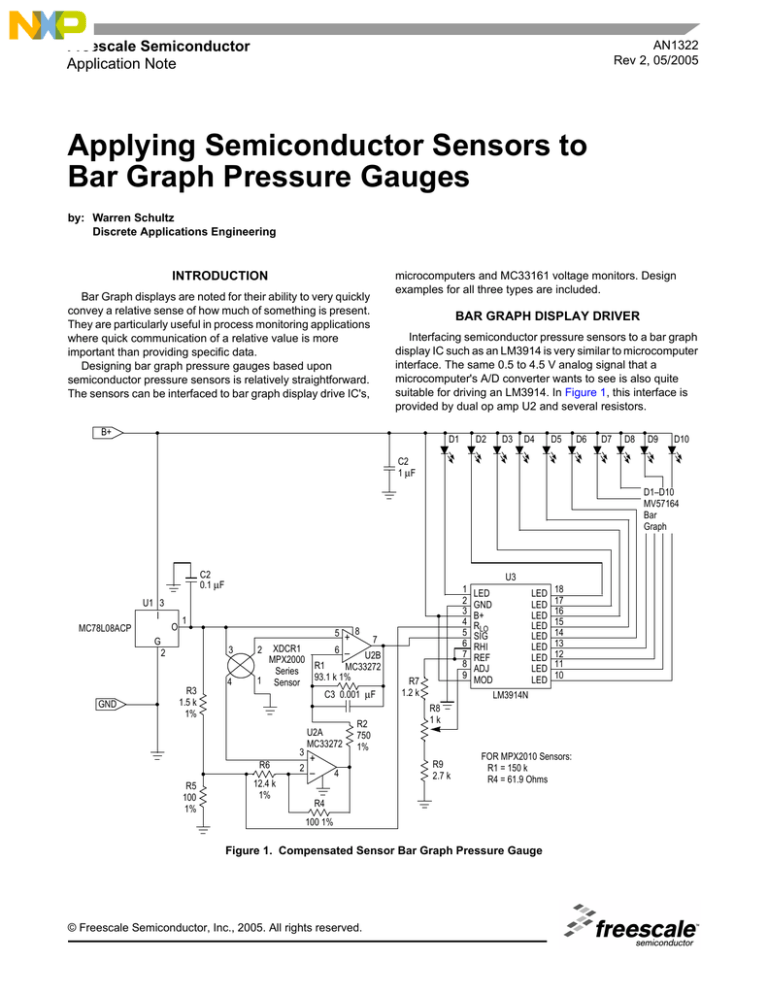
suitable for driving an LM3914. In Figure 1, this interface is
provided by dual op amp U2 and several resistors.
B+
D1
D2
D3
D4
D5
D6
D7
D8
D9
D10
C2
1 µF
D1–D10
MV57164
Bar
Graph
C2
0.1 µF
U1 3
I
MC78L08ACP
O
1
G
3
2
GND
U3
R3
1.5 k
1%
4
5 + 8
7
XDCR1
6 –
2
U2B
MPX2000
R1
MC33272
Series
1 Sensor 93.1 k 1%
C3 0.001 µF
3
R6
R5
100
1%
12.4 k
1%
2
U2A
MC33272
+
–
R2
750
1%
4
1
2
3
4
5
6
7
8
9
R7
1.2 k
LED
GND
B+
RLO
SIG
RHI
REF
ADJ
MOD
LED
LED
LED
LED
LED
LED
LED
LED
LED
LM3914N
R8
1k
R9
2.7 k
FOR MPX2010 Sensors:
R1 = 150 k
R4 = 61.9 Ohms
R4
100 1%
Figure 1. Compensated Sensor Bar Graph Pressure Gauge
© Freescale Semiconductor, Inc., 2005. All rights reserved.
18
17
16
15
14
13
12
11
10
µA that flows into R1. The output voltage is then 4.05 V + (91
µA • 93.1k) = 12.5 V. Dividing 12.5 V by the 100 mV input
yields a gain of 125, which provides a 4.0 V span for 32 mV of
full scale sensor output.
Setting divider R3, R5 at 0.5 V results in a 0.5 V to 4.5 V
output that is easily tied to an LM3914. The block diagram that
appears in Figure 2 shows the LM3914's internal architecture.
Since the lower resistor in the input comparator chain is
pinned out at RLO, it is a simple matter to tie this pin to a
voltage that is approximately equal to the interface circuit's
0.5 V zero pressure output voltage. Returning to Figure 1, this
is accomplished by using the zero pressure offset voltage that
is generated at the output of divider R3, R5.
Again looking at Figure 1, full scale is set by adjusting the
upper comparator's reference voltage to match the sensor's
output at full pressure. An internal regulator on the LM3914
sets this voltage with the aid of resistors R7, R9, and
adjustment pot R8.
Eight volt regulated power is supplied by an MC78L08. The
LED's are powered directly from LM3914 outputs, which are
set up as current sources. Output current to each LED is
approximately 10 times the reference current that flows from
pin 7 through R7, R8, and R9 to ground. In this design it is
nominally (4.5 V/4.9 k)10 = 9.2 mA.
The op amp interface amplifies and level shifts the sensor's
output. To see how this amplifier works, simplify it by
grounding the output of voltage divider R3, R5. If the common
mode voltage at pins 2 and 4 of the sensor is 4.0 V, then pin 2
of U2A and pin 6 of U2B are also at 4.0 V. This puts 4.0 V
across R6. Assuming that the current in R4 is equal to the
current in R6, 323 µA • 100 ohms produces a 32 mV drop
across R4 which adds to the 4.0 V at pin 2. The output voltage
at pin 1 of U2A is, therefore, 4.032 V. This puts 4.032 - 4.0 V
across R2, producing 43 µA. The same current flowing
through R1 again produces a voltage drop of 4.0 V, which sets
the output at zero. Substituting a divider output greater than
zero into this calculation reveals that the zero pressure output
voltage is equal to the output voltage of divider R3, R5. For
this DC output voltage to be independent of the sensor's
common mode voltage, it is necessary to satisfy the condition
that R1/R2 = R6/R4.
Gain can be determined by assuming a differential output
at the sensor and going through the same calculation. To do
this assume 100 mV of differential output, which puts pin 2 of
U2A at 3.95 V, and pin 6 of U2B at 4.05 V. Therefore, 3.95 V
is applied to R6, generating 319 µA. This current flowing
through R4 produces 31.9 mV, placing pin 1 of U2A at
3950 mV + 31.9 mV = 3982 mV. The voltage across R2 is then
4050 mV - 3982 mV = 68 mV, which produces a current of 91
Comparator
1 OF 10
LM391
–
4
+
10
1k
–
+
11
1k
–
+
12
1k
–
+
13
1k
–
+
14
1k
–
+
15
1k
–
+
16
1k
–
+
17
1k
–
+
18
1k
–
+
1
RHI 6
REF
OUT
This Load
Determines
LED
Brightness
7+
Reference
Voltage
Source
1.25 V
8
REF
ADJ
V+
3
RLO
4
SIG 5 20 k
IN
1k
V+
–
Buffer
+
LED
V+
From
Pin 11
Mode
Select
Amplifier
V–
9
2
Controls
Type of
Display Bar
or Single
LED
Figure 2. LM3914 Block Diagram
AN1322
2
Sensors
Freescale Semiconductor
+12 V
D1
D2
D3
D4
D5
D6
D7
D8
D9
D10
C2
1 µF
U1
C1
0.1 µF
U3 3
I
MC78L05ACP
O
1
2
3
4
5
6
7
8
9
1
G
3
2
R4
1.3 k
2
1
U2
MPX5100
GND
R2
1.2 k
LED
LED
LED
LED
LED
LED
LED
LED
LED
LED
GND
B+
RLO
SIG
RHI
REF
ADJ
MOD
18
17
16
15
14
13
12
11
10
LM3914
R5
1k
R6
100
Full Scale Cal.
R3
2.7 k
R1
100
Figure 3. MPX5100 Bar Graph Pressure Gauge
Over a zero to 50°C temperature range combined accuracy
for the sensor, interface, and driver IC are ±10%. Given a 10
segment display total accuracy for the bar graph readout is
approximately ± (10 kPa +10%).
This circuit can be simplified by substituting an MPX5100
integrated sensor for the MPX2100 and the op amp interface.
The resulting schematic is shown in Figure 3. In this case zero
reference for the bar graph is provided by dividing down the
5 V regulator with R4, R1 and adjustment pot R6. The voltage
at the wiper of R6 is adjusted to match the sensor's zero
pressure offset voltage. It is connected to RLO to zero the bar
graph.
MICROCOMPUTER BAR GRAPH
Microcomputers with internal A/D converters such as an
MC68HC05B5 lend themselves to easily creating bar graphs.
Using the A/D converter to measure the sensor's analog
output voltage and output ports to individually switch LED's
makes a relatively straightforward pressure gauge. This type
of design is facilitated by a new MDC4510A gated current
sink. The MDC4510A takes one of the processor's logic
outputs and switches 10 mA to an LED. One advantage of this
approach is that it is very flexible regarding the number of
segments that are used, and has the availability through
software to independently adjust scaling factors for each
segment. This approach is particularly useful for process
monitoring in systems where a microprocessor is already in
place.
Figure 4 shows a direct connection from an MPX5100
sensor to the microcomputer. Similar to the previous example,
an MPX2000 series sensor with the op amp interface that is
shown in Figure 1 can be substituted for the MPX5100. In this
case the op amp interface's output at pin 7 ties to port PD5,
and its supply needs to come from a source greater than
6.5 V.
AN1322
Sensors
Freescale Semiconductor
3
+5
VRL
VRH
D/A
TCAP1
TCAP2
VDD
PD0
PD1
PD2
PD3
PD4
VPP6
IRQ
PD5
XDCR1
MPX5100
R1
10 k
J1
R4
10 M
C2
22 pF
D5
MV53214A
MV54124A
MV54124A
MV54124A
MV57124A
I2
MDC4510A
PC2
I3
MDC4510A
R2
U2
10 k
MC34064P-5
J2
D4
PC1
2
C1
22 pF
D3
I1
MDC4510A
U1
MC68HC705B5FN
R3
4.7 k
D2
PC0
1
3
D1
RESET
Y1
4 MHz
PC3
I4
MDC4510A
PD6
PD7
OSC1
OSC2
VSS
PC4
I5
MDC4510A
RDI
TDO
Figure 4. Microcomputer Bar Graph Pressure Gauge
PROCESS MONITOR
For applications where an inexpensive HIGH-LOW-OK
process monitor is required, the circuit in Figure 5 does a good
job. It uses an MC33161 Universal Voltage Monitor and the
same analog interface previously described to indicate high,
low or in-range pressure.
A block diagram of the MC33161 is illustrated in Figure 6.
By tying pin 1 to pin 7 it is set up as a window detector.
Whenever input 1 exceeds 1.27 V, two logic ones are placed
at the inputs of its exclusive OR gate, turning off output 1.
Therefore this output is on unless the lower threshold is
exceeded. When 1.27 V is exceeded on input 2, just the
opposite occurs. A single logic one appears at its exclusive
OR gate, turning on output 2. These two outputs drive LED's
through MDC4010A 10 mA current sources to indicate low
pressure and high pressure.
Returning to Figure 5, an in-range indication is developed
by turning on current source I1 whenever both the high and
low outputs are off. This function is accomplished with a
discrete gate made from D1, D2 and R7. Its output feeds the
input of switched current source I1, turning it on with R7 when
neither D1 nor D2 is forward biased.
Thresholds are set independently with R8 and R9. They
sample the same 4.0 V full scale span that is used in the other
examples. However, zero pressure offset is targeted for 1.3 V.
This voltage was chosen to approximate the 1.27 V reference
at both inputs, which avoids throwing away the sensor's
analog output signal to overcome the MC33161's input
threshold. In addition, R10 and R11 are selected such that at
full scale output, i.e., 5.3 V on pin 7, the low side of the pots is
nominally at 1.1 V. This keeps the minimum input just below
the comparator thresholds of 1.27 V, and maximizes the
resolution available from adjustment pots R8 and R9. When
level adjustment is not desired, R8 - R11 can be replaced by
a simpler string of three fixed resistors.
AN1322
4
Sensors
Freescale Semiconductor
B+
I2
1 MDC4010A
1
I3
MDC4010A
C1
0.1 µF
2
2 D6
D5
D4
MV53124A MV54124A MV57124A
HIGH
0k
LOW
C2
0.1 µF
U1 3
I
G
MC78L08ACP 2
O
1
XDCR1
MPX2000
Series
Sensor
2
3
GND
R5
1.33 k
1%
4
R6
11.3 k
1%
1
R4
100
1%
2
D2
1N914
C3 0.001 µF
U2A
MC33272
3
+
1
2 –
4
3
D1
1N914
R1 93.1 k 1%
R3
6.65 k
1%
I1
1 MDC4510A
R7
7.5 k
5 + 8
7
6 –
U2B
MC33272
R2
750
1%
R8
10 k
LOW
R10
2.7 k
R9
10 k
HI
U3
1 REF
VCC
2 IN1
MODE
3 IN2
OUT1
4
GND
OUT2
MC33161
8
7
6
5
R11
2.7 k
Figure 5. An Inexpensive Three-Segment Processor Monitor
AN1322
Sensors
Freescale Semiconductor
5
1
7
VREF
2.54 V
Reference
Mode Select
–
+
VCC
Out 1
8
6
2.8 V
2
Input 1
+
–
1.27 V
–
+
Out 2
5
0.6 V
3
Input 2
+
–
1.27 V
GND
4
Figure 6. MC33161 Block Diagram
CONCLUSION
The circuits that have been shown here are intended to
make simple, practical and cost effective bar graph pressure
gauges. Their application involves a variety of trade-offs that
can be matched to the needs of individual applications. In
general, the most important trade-offs are the number of
segments required and processor utilization. If the system in
which the bar graph is used already has a microprocessor with
unused A/D channels and I/O ports, tying MDC4510A current
sources to the unused output ports is a very cost effective
solution. On a stand-alone basis, the MC33161 based
process monitor is the most cost effective where only 2 or 3
segments are required. Applications that require a larger
number of segments are generally best served by one of the
circuits that uses a dedicated bar graph display.
REFERENCES
1. Alberkrack, Jade, & Barrow, Stephen; “Power Supply
Monitor IC Fills Voltage Sensing Roles,” Power
Conversion & Intelligent Motion, October 1991.
2. Lucas, William, “An Evaluation System for Direct
Interface of the MPX5100 Pressure Sensor with a
Microprocessor,” Freescale Application Note AN1305.
3. Schultz, Warren, “Integrated Sensor Simplifies Bar
Graph Pressure Gauge,” Freescale Application Note
AN1304.
4. Schultz, Warren, “Compensated Sensor Bar Graph
Pressure Gauge,” Freescale Application Note AN1309.
AN1322
6
Sensors
Freescale Semiconductor
NOTES
AN1322
Sensors
Freescale Semiconductor
7
How to Reach Us:
Home Page:
www.freescale.com
E-mail:
support@freescale.com
USA/Europe or Locations Not Listed:
Freescale Semiconductor
Technical Information Center, CH370
1300 N. Alma School Road
Chandler, Arizona 85224
+1-800-521-6274 or +1-480-768-2130
support@freescale.com
Europe, Middle East, and Africa:
Freescale Halbleiter Deutschland GmbH
Technical Information Center
Schatzbogen 7
81829 Muenchen, Germany
+44 1296 380 456 (English)
+46 8 52200080 (English)
+49 89 92103 559 (German)
+33 1 69 35 48 48 (French)
support@freescale.com
Japan:
Freescale Semiconductor Japan Ltd.
Headquarters
ARCO Tower 15F
1-8-1, Shimo-Meguro, Meguro-ku,
Tokyo 153-0064
Japan
0120 191014 or +81 3 5437 9125
support.japan@freescale.com
Asia/Pacific:
Freescale Semiconductor Hong Kong Ltd.
Technical Information Center
2 Dai King Street
Tai Po Industrial Estate
Tai Po, N.T., Hong Kong
+800 2666 8080
support.asia@freescale.com
For Literature Requests Only:
Freescale Semiconductor Literature Distribution Center
P.O. Box 5405
Denver, Colorado 80217
1-800-441-2447 or 303-675-2140
Fax: 303-675-2150
LDCForFreescaleSemiconductor@hibbertgroup.com
AN1322
Rev. 2
05/2005
Information in this document is provided solely to enable system and software
implementers to use Freescale Semiconductor products. There are no express or
implied copyright licenses granted hereunder to design or fabricate any integrated
circuits or integrated circuits based on the information in this document.
Freescale Semiconductor reserves the right to make changes without further notice to
any products herein. Freescale Semiconductor makes no warranty, representation or
guarantee regarding the suitability of its products for any particular purpose, nor does
Freescale Semiconductor assume any liability arising out of the application or use of any
product or circuit, and specifically disclaims any and all liability, including without
limitation consequential or incidental damages. “Typical” parameters that may be
provided in Freescale Semiconductor data sheets and/or specifications can and do vary
in different applications and actual performance may vary over time. All operating
parameters, including “Typicals”, must be validated for each customer application by
customer’s technical experts. Freescale Semiconductor does not convey any license
under its patent rights nor the rights of others. Freescale Semiconductor products are
not designed, intended, or authorized for use as components in systems intended for
surgical implant into the body, or other applications intended to support or sustain life,
or for any other application in which the failure of the Freescale Semiconductor product
could create a situation where personal injury or death may occur. Should Buyer
purchase or use Freescale Semiconductor products for any such unintended or
unauthorized application, Buyer shall indemnify and hold Freescale Semiconductor and
its officers, employees, subsidiaries, affiliates, and distributors harmless against all
claims, costs, damages, and expenses, and reasonable attorney fees arising out of,
directly or indirectly, any claim of personal injury or death associated with such
unintended or unauthorized use, even if such claim alleges that Freescale
Semiconductor was negligent regarding the design or manufacture of the part.
Freescale™ and the Freescale logo are trademarks of Freescale Semiconductor, Inc.
All other product or service names are the property of their respective owners.
© Freescale Semiconductor, Inc. 2005. All rights reserved.


