Description and schematic diagram
advertisement
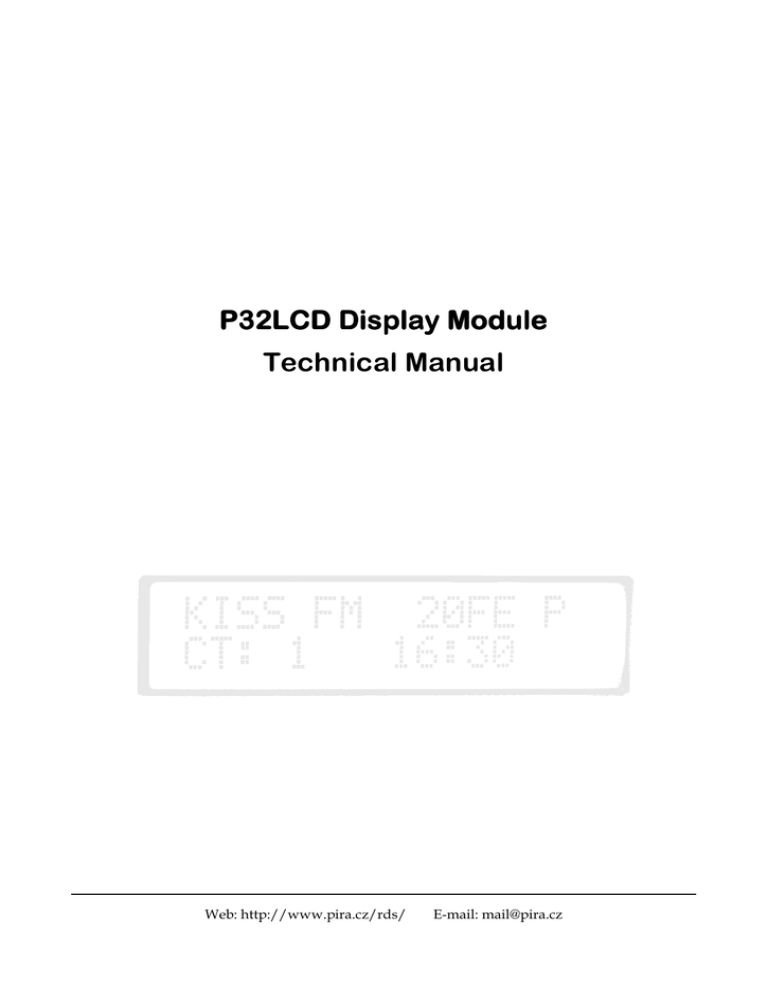
P32LCD Display Module Technical Manual Web: http://www.pira.cz/rds/ E-mail: mail@pira.cz 2 1 2 Technical Specifications Parameter Value Device kind Optional LCD module for the PIRA32 RDS Encoder Display unit Alphanumerical 16 x 2 characters, white backlight Active LCD area dimensions 66 x 16 mm Communication bus IIC 400 kHz Firmware version required 1.5b or later Character set See Annexes Power supply 5 V, common with 4-pin bus connector Supply current 40 mA Schematic Diagram 1 Adjusting elements: R2 – LCD contrast J2 – backlight on/off jumper LCD connection (J1): LCD pin 1 Vss 2 Vcc 3 Vee 4 RS 5 R/W 6 E 7 DB0 8 DB1 9 DB2 10 DB3 11 DB4 12 DB5 13 DB6 14 DB7 15 LED+ 16 LED- Connected to Ground +5 V R2 trimmer U1 pin 17 Ground U1 pin 16 Ground Ground Ground Ground U1 pin 15 U1 pin 14 U1 pin 13 U1 pin 12 +5 V through R1 Ground 3 3 PIRA32 LCD Output The LCD area is divided into two lines. The first line shows key RDS services that require quick access. These services are PS (incl. dynamic), PI, TP and TA. PS PI TP TA The second line shows the most important status values and RDS services in a loop. Depending on the configuration some values may be omitted. For example if the internal clock source is set for the RDS subcarrier, the PILOT value is not showed. Some events may affect the order. For example if Radiotext changes, it's showed in the next cycle regardless of previous order value. Status value or RDS service Meaning 1 RDSGEN ON = RDS generator enabled (1), OFF = no RDS output (0). 2 LEVEL RDS level (0 = min., 255 = max.). Showed only if appropriate support is integrated in hardware. Units with RDS level set by on-board trimmer skip this item. 3 PROGRAM Actual program bank selected. 4 PTY, MS, DI Program Type code; Music/Speech; Decoder Identification code. 5 ADR The RDS encoder address. If the unit is selected (listening for the ASCII commands), the character '*' is showed. 0,0 6 SITE The site address. 0,0 7 UECP ON = The RDS encoder accepts both ASCII and UECP commands, OFF = the RDS encoder accepts ASCII commands only. OFF 8 NOHDR ON = No header communication mode is active, OFF = standard communication mode. OFF 9 SPEED Actual RS232 port speed on which the control commands are expected. 10 PILOT ON = pilot tone present, OFF = no pilot tone. 11 CT ON = CT enabled, OFF = CT disabled; RDS encoder local time. 12 GRPSEQ First 16 items of RDS group sequence. 13 RT Actual Radiotext (sequence of 4 x 16 characters). Order Default value ON 1 022E1022EA022XYR 4 4 ANNEXES The LCD module layout and dimensions: Top side Backlight on/off Contrast adjust Pin 1 CAUTION! Special care is required when connecting the LCD module. Pin 1 of the LCD module to pin 1 of the RDS board etc. Otherwise the LCD unit may become damaged! Turn off the device before connecting the LCD module. Contour drawing, character set: 5. Contour Drawing &Block Diagram 80.0 0.5 71.2 66.0(VA) 56.2(AA) 2.5 16 31.0 5.08 11.5(AA) 25.2 16.0(VA) K 36.0 0.5 8.6 18.3 1 1 2 3 4 5 6 7 8 9 10 11 12 13 14 15 16 13.2Max 2.5 12.55 7.55 12.45 8.0 P2.54*15=38.1 3.0 1.8 16-P1.0 PTH 15.76 10.3 5.7 4.95 A 4-P1.0 2.5 40.55 4- 2.5 PTH 4- 5.0 PAD 75.0 1.6 LED B/L 3.55 2.95 0.6 0.6 0.55 0.3mm. 0.4 5.95 5.55 0.7 0.65 The non-specified tolerance of dimension is VR 10K~20K Vdd Vo Vss Vee External contrast adjustment. Com1~16 Controller/Com Driver HD44780 or Equivalent Bias and Power Circuit 80 series or 68 series RS R/W E DB0~DB7 N.V. Generator MPU DOT SIZE SCALE 5/1 16X2 LCD Seg1~40 Seg41~80 D Seg Driver M CL1 CL2 Vdd,Vss,V1~V5 Optional Character located DDRAM address DDRAM address 1 2 3 4 5 6 7 8 9 10 11 12 13 14 15 16 00 01 02 03 04 05 06 07 08 09 0A 0B 0C 0D 0E 0F 40 41 42 43 44 45 46 47 48 49 4A 4B 4C 4D 4E 4F Page 7 , Total 27 Pages Vss Vdd Vo RS R/W E DB0 DB1 DB2 DB3 DB4 DB5 DB6 DB7 A K 7. Character Generator ROM Pattern Table 2. Upper 4 bit Lower 4 bit LLLL LLLH LLHL LLHH LHLL LHLH LHHL LHHH HLLL HLLH HLHL HLHH HHLL HHLH HHHL HHHH LLLL CG RAM (1) LLLH CG RAM (2) LLHL CG RAM (3) LLHH CG RAM (4) LHLL CG RAM (5) LHLH CG RAM (6) LHHL CG RAM (7) LHHH CG RAM (8) HLLL CG RAM (1) HLLH CG RAM (2) HLHL CG RAM (3) HLHH CG RAM (4) HHLL CG RAM (5) HHLH CG RAM (6) HHHL CG RAM (7) HHHH CG RAM (8) Page 11 , Total 27 Pages
