NJW4615A
advertisement

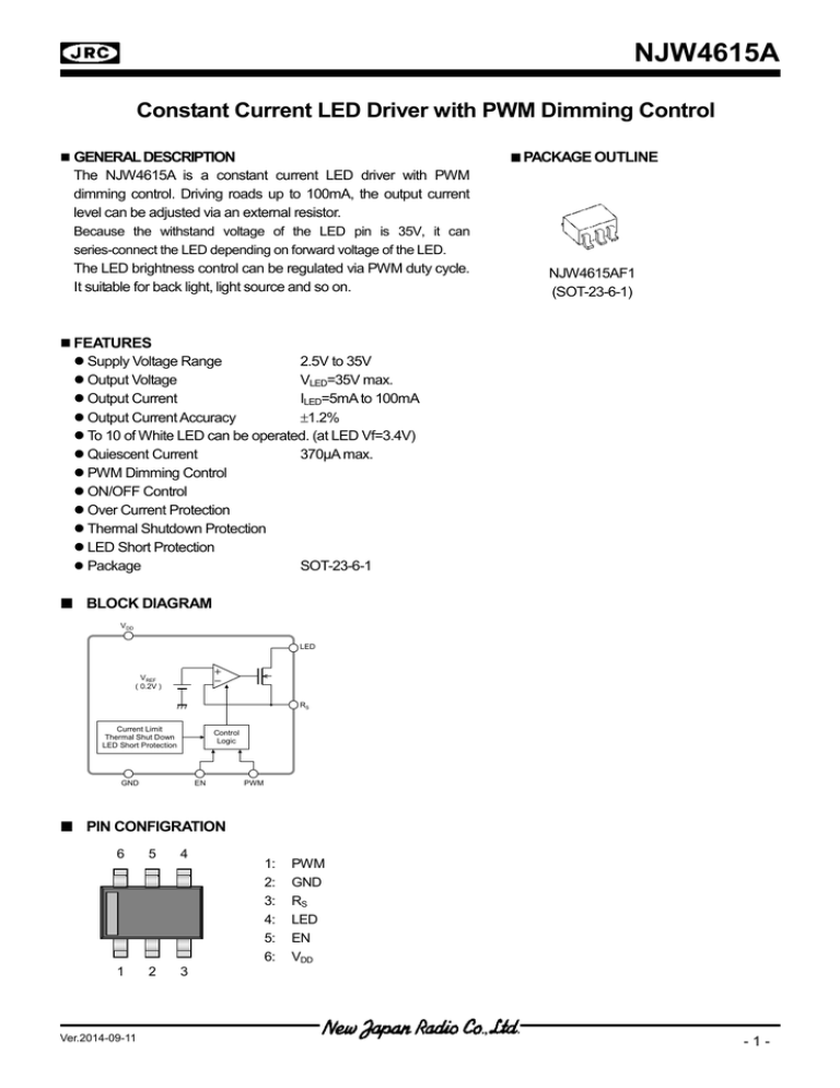
NJW4615A Constant Current LED Driver with PWM Dimming Control GENERAL DESCRIPTION PACKAGE OUTLINE The NJW4615A is a constant current LED driver with PWM dimming control. Driving roads up to 100mA, the output current level can be adjusted via an external resistor. Because the withstand voltage of the LED pin is 35V, it can series-connect the LED depending on forward voltage of the LED. The LED brightness control can be regulated via PWM duty cycle. It suitable for back light, light source and so on. NJW4615AF1 (SOT-23-6-1) FEATURES Supply Voltage Range 2.5V to 35V Output Voltage VLED=35V max. Output Current ILED=5mA to 100mA Output Current Accuracy 1.2% To 10 of White LED can be operated. (at LED Vf=3.4V) Quiescent Current 370µA max. PWM Dimming Control ON/OFF Control Over Current Protection Thermal Shutdown Protection LED Short Protection Package SOT-23-6-1 BLOCK DIAGRAM VDD LED VREF ( 0.2V ) RS Current Limit Thermal Shut Down LED Short Protection Control Logic GND EN PWM PIN CONFIGRATION 6 5 4 1 2 3 Ver.2014-09-11 1: 2: 3: 4: 5: 6: PWM GND RS LED EN VDD -1- NJW4615A ABSOLUTE MAXIMUM RATINGS PARAMETERS SYMBOL Supply Voltage VDD Output voltage VLED EN Pin Voltage VEN PWM Pin Voltage VPWM Power Dissipation PD Junction Temperature Range Operating Temperature Range Storage Temperature Range Tj Topr Tstg RATINGS -0.3 to +40 -0.3 to +40 -0.3 to +40 -0.3 to +6 510 (*1) 710 (*2) -40 to +150 -40 to +125 -50 to +150 (Ta=25C) UNIT V V V V mW C C C (*1): Mounted on glass epoxy board. (76.2×114.3×1.6mm: based on EIA/JEDEC standard, 2Layers) (*2): Mounted on glass epoxy board. (76.2×114.3×1.6mm: based on EIA/JEDEC standard, 4Layers), Internal Cu area: 74.2×74.2mm RECOMMENDED OPERATING CONDITIONS PARAMETERS SYMBOL Supply Voltage VDD Output Current ILED Output Voltage VLED CONDITIONS MIN 2.5 5 - TYP - (Ta=25C) MAX Unit 35 V 100 mA 35 V ELECTRICAL CHARACTERISTICS (Unless otherwise noted, VDD= VEN=12V, VLED=1V, RS=10Ω, VPWM=OPEN, Ta=25C) PARAMETERS SYMBOL CONDITIONS MIN TYP MAX Unit Quiescent Current IDD 260 370 µA Quiescent Current at OFF State IDD_OFF VEN=GND 0.1 µA Output Current Accuracy -1.2 +1.2 % ILED Output Pin Leak Current 1 ILEAK1 VEN=GND, VDD =35V, VLED =35V 0.1 µA Output Pin Leak Current 2 ILEAK2 VPWM=GND VDD =35V, VLED =35V 0.1 µA V EN Pin ON Voltage VEN_ON 1.6 VDD ILED=OFFON V EN Pin OFF Voltage VEN_OFF 0 0.3 ILED=ONOFF V PWM Pin ON Voltage 1 VPWM_ON 1 VDD < 5V, ILED = OFF ON 0.7VDD VDD V PWM Pin OFF Voltage 1 VPWM_OFF 1 VDD < 5V, ILED = ON OFF 0 0.3VDD V PWM Pin ON Voltage 2 VPWM_ON 2 VDD 5V, ILED = OFF ON 3.5 5.5 V PWM Pin OFF Voltage 2 VPWM_OFF 2 VDD 5V, ILED = ON OFF 0 1.5 EN Pin Input Current IEN VEN = 12V 7 µA PWM Pin Pull Up Resistance RPWM 1 MΩ RS Pin Output Current IOUT_RS LED = OPEN 2.3 µA 3 PWM Pin ON Delay Time tPWM_ON µs VPWM = L H, ILED = OFF ON 1 PWM Pin OFF Delay Time tPWM_OFF µs VPWM = H L, ILED = ON OFF LED Short Protection VLED_SHORT 17 20 23 V Detect Voltage Maximum Output Current ILED_MAX RS = 0 Ω 100 170 mA -2- Ver.2014-09-11 NJW4615A TYPICAL APPLICATION VDD VDD ILED LED 0 ILED VREF ( 0.2V ) RS RS : Current Sense Resistance Current Limit Thermal Shut Down LED Short Protection GND Control Logic EN PWM H : ON L : OFF Dimming Control at PWM Signal or Light ON at Open The Rs Resistance Setting formula: RS ( ) 0.2(V ) ILED ( A) PIN DESCRIPTIONS Pin No. Pin Name I/O 1 PWM I PWM Signal input pin for Dimming Control. Not use Dimming Control, This pin is open. 2 GND - Ground 3 RS O ILED Setting Resistor Connect Pin. The LED current can be set connecting resistance (RS) between RS pin and GND pin. RS [Ω] = 0.2 [V] / ILED [A] 4 LED O Constant Current Circuit Output Pin Connect Cathode Pin of LED. 5 EN I Standby Control Pin Normal Operation at the time of High Level. Standby Mode at the time of Low Level. 6 VDD I Power Supply Ver.2014-09-11 Function -3- NJW4615A MEMO [CAUTION] The specifications on this databook are only given for information, without any guarantee as regards either mistakes or omissions. The application circuits in this databook are described only to show representative usages of the product and not intended for the guarantee or permission of any right including the industrial rights. -4- Ver.2014-09-11
