Stepped Impedance Key-shaped Resonator for Bandpass
advertisement

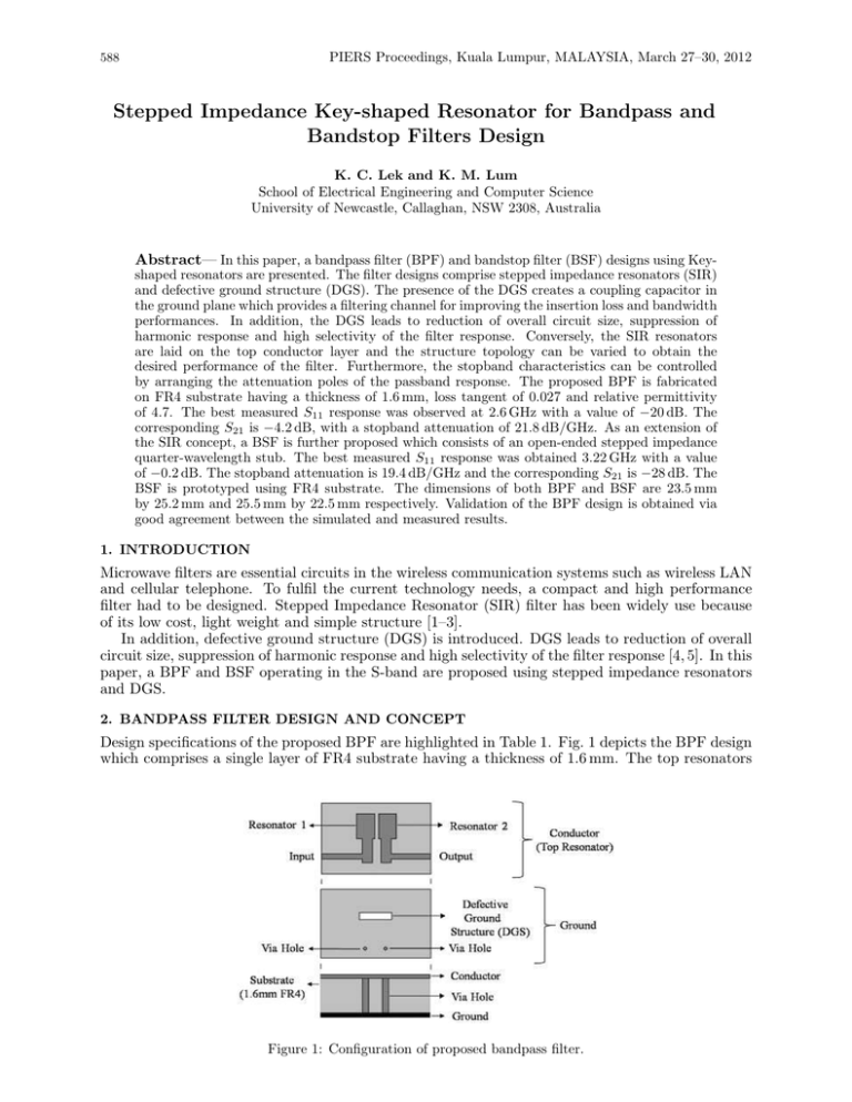
PIERS Proceedings, Kuala Lumpur, MALAYSIA, March 27–30, 2012 588 Stepped Impedance Key-shaped Resonator for Bandpass and Bandstop Filters Design K. C. Lek and K. M. Lum School of Electrical Engineering and Computer Science University of Newcastle, Callaghan, NSW 2308, Australia Abstract— In this paper, a bandpass filter (BPF) and bandstop filter (BSF) designs using Keyshaped resonators are presented. The filter designs comprise stepped impedance resonators (SIR) and defective ground structure (DGS). The presence of the DGS creates a coupling capacitor in the ground plane which provides a filtering channel for improving the insertion loss and bandwidth performances. In addition, the DGS leads to reduction of overall circuit size, suppression of harmonic response and high selectivity of the filter response. Conversely, the SIR resonators are laid on the top conductor layer and the structure topology can be varied to obtain the desired performance of the filter. Furthermore, the stopband characteristics can be controlled by arranging the attenuation poles of the passband response. The proposed BPF is fabricated on FR4 substrate having a thickness of 1.6 mm, loss tangent of 0.027 and relative permittivity of 4.7. The best measured S11 response was observed at 2.6 GHz with a value of −20 dB. The corresponding S21 is −4.2 dB, with a stopband attenuation of 21.8 dB/GHz. As an extension of the SIR concept, a BSF is further proposed which consists of an open-ended stepped impedance quarter-wavelength stub. The best measured S11 response was obtained 3.22 GHz with a value of −0.2 dB. The stopband attenuation is 19.4 dB/GHz and the corresponding S21 is −28 dB. The BSF is prototyped using FR4 substrate. The dimensions of both BPF and BSF are 23.5 mm by 25.2 mm and 25.5 mm by 22.5 mm respectively. Validation of the BPF design is obtained via good agreement between the simulated and measured results. 1. INTRODUCTION Microwave filters are essential circuits in the wireless communication systems such as wireless LAN and cellular telephone. To fulfil the current technology needs, a compact and high performance filter had to be designed. Stepped Impedance Resonator (SIR) filter has been widely use because of its low cost, light weight and simple structure [1–3]. In addition, defective ground structure (DGS) is introduced. DGS leads to reduction of overall circuit size, suppression of harmonic response and high selectivity of the filter response [4, 5]. In this paper, a BPF and BSF operating in the S-band are proposed using stepped impedance resonators and DGS. 2. BANDPASS FILTER DESIGN AND CONCEPT Design specifications of the proposed BPF are highlighted in Table 1. Fig. 1 depicts the BPF design which comprises a single layer of FR4 substrate having a thickness of 1.6 mm. The top resonators Figure 1: Configuration of proposed bandpass filter. Progress In Electromagnetics Research Symposium Proceedings, KL, MALAYSIA, March 27–30, 2012 589 1 and 2 are laid on the FR4 substrate. The structure of the resonators can be varied to obtain the desired performance of the filter. Furthermore, the stopband characteristics of the BPF can be controlled by arranging the attenuation poles of the passband response [6, 7]. 3. BANDPASS FILTER SIMULATION AND MEASUREMENT RESULT Figure 2 detailed the dimensional data of the proposed BPF. Advanced Design System (ADS) simulation software was used to simulate the BPF design. Fig. 3 shows the simulated S11 and S21 results of the proposed BPF. The best match for the BPF is obtained at 2.62 GHz with a S11 value of less than −25 dB. In the passband response, the corresponding S21 is approximately −3 dB with an attenuation of 26.5 dB/GHz. The proposed BPF was fabricated on FR4 substrate as shown in Fig. 4. Measurements were carried out using Network Analyzer. As presented in Fig. 5, the best measured S11 was observed at 2.6 GHz with a value of −20 dB. The corresponding S21 is −4.2 dB, with a stopband attenuation of 21.8 dB/GHz. The measured −5 dB bandwidth over the passband is about 200 MHz. It is evident that the measured result agrees well with the simulation results. Table 1: Design specifications of bandpass filter. Key Parameter Operating Frequency (GHz) Return Loss, S11 (dB) Passband Insertion loss, S21 (dB) Passband (MHz) at −5 dB Stopband Attenuation Value 2.6 < −10 > −10 200 > 20 dB/GHz (a) (b) Figure 2: Key dimensional data of (a) top resonator and (b) defected ground plane. (a) Figure 3: Simulated S11 and S21 response of bandpass filter. (b) Figure 4: Fabricated bandpass filter. (a) Top resonators. (b) Ground plane. 590 PIERS Proceedings, Kuala Lumpur, MALAYSIA, March 27–30, 2012 Figure 5: Simulated and measured S11 and S21 response of bandpass filter. Table 2: Design specifications of bandstop filter. Key Parameter Operating Frequency Return Loss Stopband Insertion Loss, S21 Stopband (MHz) at −10 dB Stopband Attenuation Value 3.2 GHz > −1 dB < −10 dB 2000 > 10 dB/GHz Figure 6: Key dimensional data of top resonator. 4. BANDSTOP FILTER DESIGN AND CONCEPT As an extension of the SIR concept, a BSF is proposed. Design specifications of the proposed BPF are highlighted in Table 2. As shown in Fig. 6, the BSF design consists of an open-ended stepped impedance quarter-wavelength stub which comprises two characteristic impedances (Z1 , Z2 ) and electrical lengths (Q1 , Q2 ) that leads to the resonating of two different frequencies (wf and wc ). As illustrated in Fig. 7, the components encircled indicate the resonate circuits of the filter at frequencies wf and wc . At the resonant frequencies, wf and wc , the circuits are able to exhibit a stopband response that rejects unwanted signal thus enabling the filter to operate as a BSF [8–10]. 5. BANDSTOP SIMULATION AND MEASUREMENT RESULT Figure 8 shows the simulated S11 and S21 response of the proposed BSF. The best return loss, S11 for the BSF is obtained at 3.28 GHz with a corresponding S11 value of −0.1 dB. The stopband attenuation is 17.4 dB/GHz. In the stopband response, S21 is approximately −38 dB. The proposed BSF was prototyped using one FR4 substrate with the SMA connectors soldered onto the microstrip feed line as shown in Fig. 9. Measurements were carried out using Network Analyzer. As presented in Fig. 10, the best measured S11 was obtained at 3.22 GHz with a value of Progress In Electromagnetics Research Symposium Proceedings, KL, MALAYSIA, March 27–30, 2012 591 (a) (b) Figure 7: Equivalent circuit of (a) configuration of stepped impedance resonator, (b) bandstop filter. (a) Figure 8: Simulated S11 and S21 response of bandstop filter. (b) Figure 9: Fabricated bandstop filter. (a) Top resonator. (b) Ground plane. Figure 10: Simulated and measured S11 and S21 response of bandstop filter. −0.2 dB. The stopband attenuation is 19.4 dB/GHz and the corresponding S21 is −28 dB. The measured −10 dB bandwidth over the stopband is about 1800 MHz. Despite of the slight variance in the results due to unexpected fabrication tolerance, material losses and parasitic effect of the SMA connectors, it is evident that the measured result agrees well with the simulation results. 6. CONCLUSION The design of a bandpass filter based on the configuration of stepped impedance key-shaped resonators with defected ground structure has been validated through simulation and practical measurement. It has also been demonstrated that the stepped impedance key-shaped resonator topology of the proposed bandpass filter design can be further modified to obtain a bandstop filter response. The proposed filters have the advantages of providing reasonably acceptable filtering function using simple resonator and defected ground structure topology and are easy to be fabricated. The proposed configuration seems particularly suitable for use in multilayer transceiver designs [11–14] and localization applications [15–18]. 592 PIERS Proceedings, Kuala Lumpur, MALAYSIA, March 27–30, 2012 REFERENCES 1. Zhang, J., J.-Z. Gu, B. Cui, and X.-W. Sun. “Compact and harmonic suppression open-loop resonator bandpass filter with tri-section sir,” Progress In Electromagnetics Research, Vol. 69, 93–100, 2007. 2. Velazquez-Ahumada, M. D. C., J. Martel, F. Medina, and F. Mesa, “Application of stub loaded folded stepped impedance resonators to dual band filter design,” Progress In Electromagnetics Research, Vol. 102, 107–124, 2010. 3. Liu, Y., W. B. Dou, and Y.-J. Zhao, “A tri-band bandpass filter realized using tri-mode t-shape branches,” Progress In Electromagnetic Research, Vol. 105, 425–444, 2010. 4. Lin, W.-J., C.-S. Chang, J.-Y. Li, D.-B. Lin, L.-S. Chen, and M.-P. Houng, “A new approach of dual-band filters by stepped impedance simplified cascaded quadruplet resonators with slot coupling,” Progress In Electromagnetic Research letters, Vol. 9, 19–28, 2009. 5. Zhang, J., J.-Z. Gu, B. Cui, and X. W. Sun, “Compact and harmonic suppression open-loop resonator bandpass filter with tri-section sir,” Progress In Electromagnetic Research, Vol. 69, 93–100, 2007. 6. Bahrami, H., M. Hakkak, and A. Pirhadi, “Analysis and design of highly compact bandpass waveguide filter using complementary split ring resonators (CSRR),” Progress In Electromagnetics Research, Vol. 80, 107–122, 2008. 7. Yang, X., Y. Fan, B. Zhang, and M. Zhao, “A novel compact suspended double side CMRC millimeter bandpass filter with wide stopband,” Progress In Electromagnetics Research Letters, Vol. 21, 59–66, 2011. 8. Yang, R.-Y., M.-H. Weng, C.-Y. Hung, H.-J. Chen, and M.-P. Houng, “Novel compact microstrip interdigital bandstop filter,” IEEE Transactions Ultrasonics, Ferroelectrics, and Frequency Control, Vol. 51, No. 8, Aug. 2004. 9. Guo, L., Z.-Y. Yu, and L. Zhang, “Design of a dual-mode dual-band filter using stepped impedance resonators,” Progress In Electromagnetics Research Letters, Vol. 14, 147–154, 2010. 10. Chin, K.-S. and C.-K. Lung, “Miniaturized microstrip dual-band bandstop filters using trisection stepped-impedance resonators,” Progress In Electromagnetics Research C, Vol. 10, 37– 48, 2009. 11. Lum, K. M., C. Laohapensaeng, and C. E. Free, “A novel traveling-wave feed technique for circularly polarized planar antennas,” IEEE Micro. and Wireless Components Letters, Vol. 15, No. 3, 180–182, Mar. 2005. 12. Lum, K. M., T. Tick, C. Free, and H. Jantunen, “Design and measurement data for a microwave CP antenna using a new travelling-wave feed concept,” European Microwave Conf., Paris, France, Oct. 2005. 13. Lum, K. M. and C. Free, “A novel traveling-wave feed technique for circularly polarized planar microstrip antennas,” IEEE Antennas and Propag. International Symposium, Vol. 2A, 250– 253, Oct. 2005. 14. Lum, K. M. and C. E. Free, “A novel dual circularly polarized planar and multi-layer LTCC antenna arrays using traveling-wave feed system,” IEEE Trans. Micro. Theory Tech., Vol. 54, No. 6, 2880–2886, Jun. 2006. 15. Seow, C. K. and S. Y. Tan, “Non line of sight localization in multipath environment,” IEEE Trans. Mobile Computing, Vol. 7, No. 5, 647–660, May 2008. 16. Seow, C. K. and S. Y. Tan, “Localization of omni-directional mobile device in multipath environments,” Progress In Electromagnetic Research, Vol. 85, 323–348, 2008. 17. Seow, C. K. and S. Y. Tan, “Localisation of mobile device in multipath environment using bi-directional estimation,” Electronics Letters, Vol. 44, No. 7, 485–487, Mar. 2008. 18. Seow, C. K. and S. Y. Tan, “Non-line-of-sight unidirectional mobile localisation in multipath environment,” Electronics Letters, Vol. 44, No. 2, 141–142, Jan. 2008.


